6116LA70 데이터 시트보기 (PDF) - Integrated Device Technology
부품명
상세내역
제조사
6116LA70 Datasheet PDF : 10 Pages
| |||
IDT6116SA/LA
CMOS STATIC RAM 16K (2K x 8-BIT)
MILITARY AND COMMERCIAL TEMPERATURE RANGES
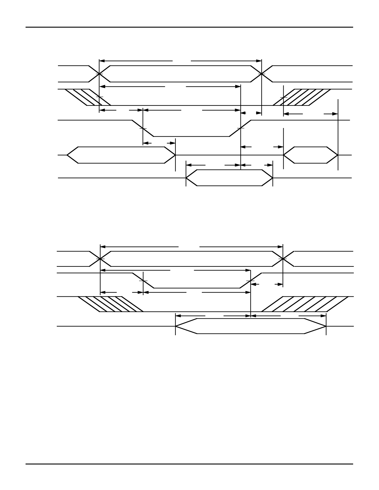
TIMING WAVEFORM OF WRITE CYCLE NO. 1, (WE CONTROLLED TIMING) (1, 2, 5, 7)
tWC
ADDRESS
CS
tAW
tAS
tWP(7)
(3)
tWR
tCHZ (6)
WE
DATA OUT
DATA IN
tWHZ(6)
PREVIOUS DATA VALID (4)
(6)
tOW
tDW
tDH
DATA VALID
DATA (4)
VALID
3089 drw 09
TIMING WAVEFORM OF WRITE CYCLE NO. 2, (CS CONTROLLED TIMING) (1, 2, 3, 5, 7)
tWC
ADDRESS
tAW
CS
(3)
tWR
tAS
tCW
WE
tDW
tDH
DATA IN
DATA VALID
3089 drw 10
NOTES:
1. WE or CS must be HIGH during all address transitions.
2. A write occurs during the overlap of a LOW CS and a LOW WE.
3. tWR is measured from the earlier of CS or WE going HIGH to the end of the write cycle.
4. During this period, the I/O pins are in the output state and the input signals must not be applied.
5. If the CS LOW transition occurs simultaneously with or after the WE LOW transition, the outputs remain in the high-impedance state.
6. Transition is measured ±500mV from steady state.
7. OE is continuously HIGH. If OE is LOW during a WE controlled write cycle, the write pulse width must be the larger of tWP or (tWHZ + tDW) to allow the
I/O drivers to turn off and data to be placed on the bus for the required tDW. If OE is HIGH during a WE controlled write cycle, this requirement does not
apply and the write pulse is the specified tWP. For a CS controlled write cycle, OE may be LOW with no degradation to tCW.
5.1
9
Share Link: 