IDT71256SA15P 데이터 시트보기 (PDF) - Integrated Device Technology
부품명
상세내역
제조사
IDT71256SA15P Datasheet PDF : 6 Pages
| |||
IDT71256SA
CMOS STATIC RAM 256K (32K x 8-BIT)
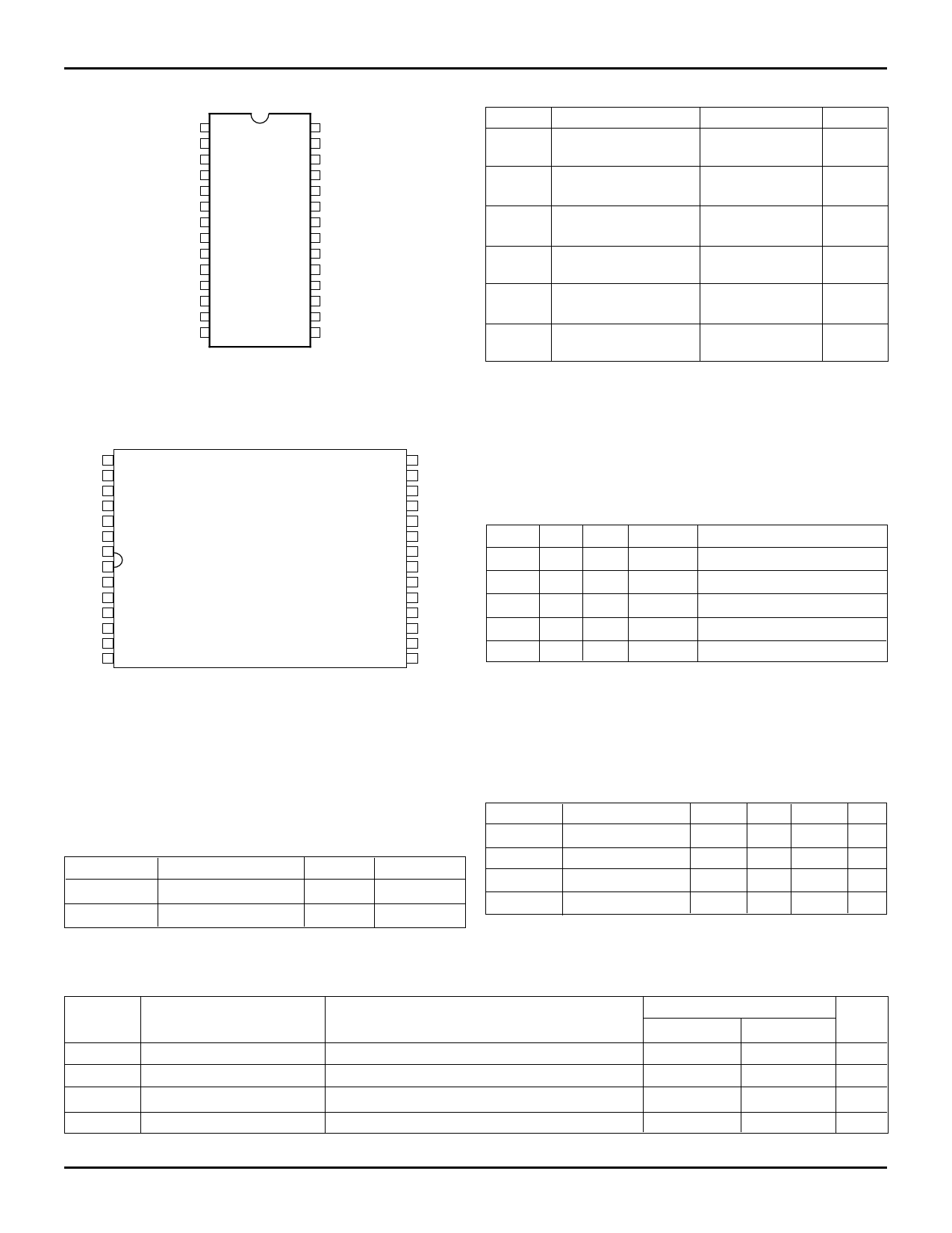
PIN CONFIGURATIONS
A14
A12
A7
A6
A5
A4
A3
A2
A1
A0
I/O0
I/O1
I/O2
GND
1
28
2
27
3
26
4
25
5
24
6
23
7
SO28-5
P28-2
22
8 P28-1 21
9
20
10
19
11
18
12
17
13
16
14
15
VCC
WE
A13
A8
A9
A11
OE
A10
CS
I/O7
I/O6
I/O5
I/O4
I/O3
2948 drw 02
DIP/SOJ
TOP VIEW
OE
22
A 11
23
A9
24
A8
25
A 13
26
WE
27
V CC
28
A 14 1
A 12 2
A7 3
A6 4
A5 5
A4 6
A3 7
SO28-8
TSOP
TOP VIEW
INDUSTRIAL AND COMMERCIAL TEMPERATURE RANGES
21 A 10
20 CS
19 I/O7
18 I/O6
17 I/O5
16 I/O4
15 I/O3
14 GND
13 I/O2
12 I/O1
11 I/O0
10 A 0
9 A1
8 A2
2948 drw 11
ABSOLUTE MAXIMUM RATINGS(1)
Symbol
Rating
Value
Unit
VCC Supply Voltage
Relative to GND
–0.5 to +7.0
V
VTERM Terminal Voltage
Relative to GND
–0.5 to VCC+0.5
V
TBIAS Temperature
Under Bias
–55 to +125
°C
TSTG
Storage
Temperature
–55 to +125
°C
PT Power
Dissipation
1.0
W
IOUT
DC Output
Current
50
mA
NOTES:
2948 tbl 02
1. Stresses greater than those listed under ABSOLUTE MAXIMUM
RATINGS may cause permanent damage to the device. This is a stress
rating only and functional operation of the device at these or any other
conditions above those indicated in the operational sections of this
specification is not implied. Exposure to absolute maximum rating
conditions for extended periods may affect reliability.
TRUTH TABLE(1,2)
CS
OE
WE
I/O
L
L
H DATAOUT
L
X
L DATAIN
L
H
H High-Z
H
X
X High-Z
VHC(3) X
X High-Z
NOTES:
1. H = VIH, L = VIL, x = Don't care.
2. VLC = 0.2V, VHC = VCC –0.2V.
3. Other inputs ≥VHC or ≤VLC.
Function
Read Data
Write Data
Outputs Disabled
Deselected — Standby (ISB)
Deselected — Standby (ISB1)
2948 tbl 04
RECOMMENDED DC OPERATING
CONDITIONS
RECOMMENDED OPERATING
TEMPERATURE AND SUPPLY VOLTAGE
Grade
Temperature
GND
VCC
Commercial
Industrial
0°C to +70°C
-40°C to +85°C
0V 4.5V to 5.5V
0V 4.5V to 5.5V
3948 tbl 09
Symbol Parameter
Min. Typ. Max. Unit
VCC
Supply Voltage
4.5 5.0 5.5 V
GND
Supply Voltage
0
0
0
V
VIH
Input High Voltage 2.2 — VCC+0.5 V
VIL
Input Low Voltage –0.5(1) —
0.8
V
NOTE:
2948 tbl 01
1. VIL (min.) = –1.5V for pulse width less than 10ns, once per cycle.
DC ELECTRICAL CHARACTERISTICS
VCC = 5.0V ± 10%
IDT71256SA
Symbol
Parameter
Test Condition
Min.
Max.
Unit
|ILI|
Input Leakage Current
VCC = Max., VIN = GND to VCC
—
5
µA
|ILO|
Output Leakage Current
VCC = Max., CS = VIH, VOUT = GND to VCC
—
5
µA
VOL
Output Low Voltage
IOL = 8mA, VCC = Min.
—
0.4
V
VOH
Output High Voltage
IOH = –4mA, VCC = Min.
2.4
—
V
2948 tbl 05
2
Share Link: 