IDT7134LA55PB 데이터 시트보기 (PDF) - Integrated Device Technology
부품명
상세내역
제조사
IDT7134LA55PB Datasheet PDF : 9 Pages
| |||
IDT7134SA/LA
HIGH-SPEED 4K x 8 DUAL-PORT STATIC RAM
MILITARY AND COMMERCIAL TEMPERATURE RANGES
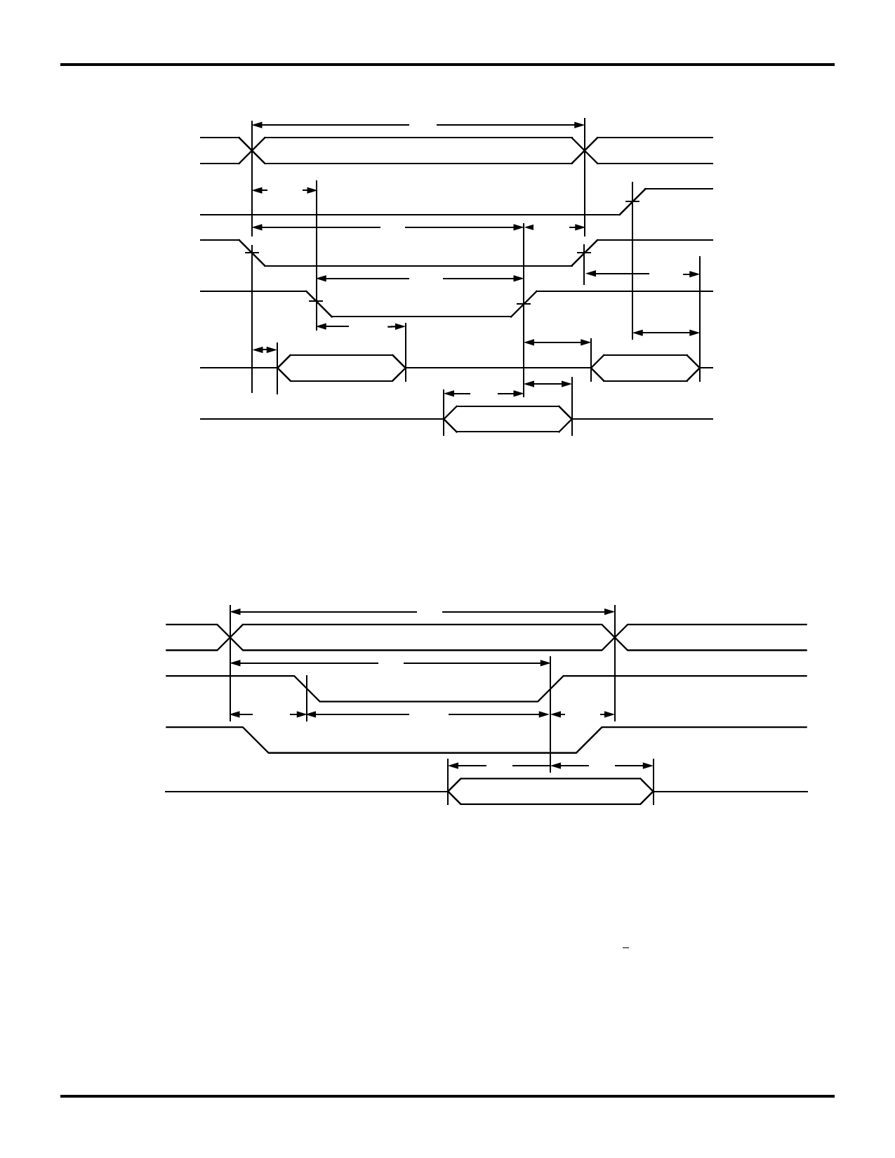
TIMING WAVEFORM OF WRITE CYCLE NO. 1, R/W CONTROLLED TIMING(1, 5, 8)
tWC
ADDRESS
OE
CE
R/W
DATAOUT
DATAIN
tAS(6)
tAW
tWR(3)
tWP(2)
tLZ
tWZ (7)
(4)
tOW
tDW
tDH
tHZ(7)
tHZ(7)
(4)
2720 drw 11
TIMING WAVEFORM OF WRITE CYCLE NO. 2, CE CONTROLLED TIMING(1, 5)
ADDRESS
CE
R/W
DATAIN
tAS(6)
tWC
tAW
tEW(2)
tDW
t1W.2R0(i3n)
tDH
2720 drw 12
NOTES:
1. R/W or CE must be High during all address transitions.
2. A write occurs during the overlap (tEW or tWP) of a CE =VIL and R/W = VIL.
3. tWR is measured from the earlier of CE or R/W going High to the end-of-write cycle.
4. During this period, the I/O pins are in the output state, and input signals must not be applied.
5. If the CE Low transition occurs simultaneously with or after the R/W Low transition, the outputs remain in the High-impedance state.
6. Timing depends on which enable signal ( CE or R/W )is asserted last.
7. This parameter is guaranteed by device characterization, but is not production tested. Transition is measured + 500mV from steady state with the Output
Test Load (Figure 2).
8. If OE is Low during a R/W controlled write cycle, the write pulse width must be the larger of tWP or (tWZ + tDW) to allow the I/O drivers to turn off data to
be placed on the bus for the required tDW. If OE is High during an R/W controlled write cycle, this requirement does not apply and the write pulse can be
as short as the specified tWP.
6.04
8
Share Link: 