IDT7164L15TPG 데이터 시트보기 (PDF) - Integrated Device Technology
부품명
상세내역
제조사
IDT7164L15TPG Datasheet PDF : 11 Pages
| |||
IDT7164S/L
CMOS Static RAM 64K (8K x 8-Bit)
Military, Commercial, and Industrial Temperature Ranges
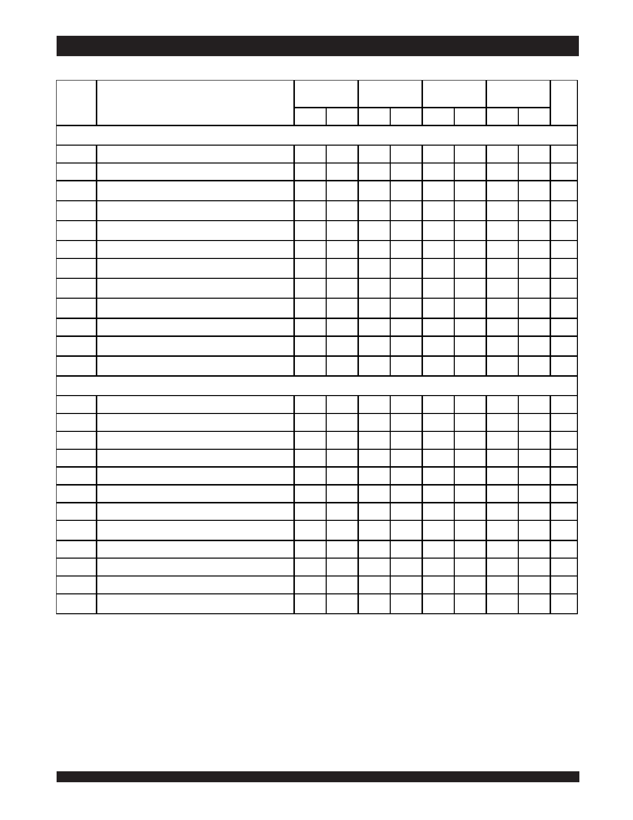
AC Electrical Characteristics (VCC = 5.0V ± 10%, All Temperature Ranges)
7164S15(1)
7164L15(1)
7164S20(2)
7164L20(2)
7164S25
7164L25
7164S35
7164L35
Symbol
Parameter
Min. Max. Min. Max. Min. Max. Min. Max. Unit
Read Cycle
tRC
Read Cycle Time
tAA
Address Access Time
15
____
20
____
25
____
35
____
ns
____
15
____
19
____
25
____
35 ns
tACS1(3) Chip Select-1 Access Time
____
15
____
20
____
25
____
35 ns
tACS2(3) Chip Select-2 Access Time
____
20
____
25
____
30
____
40 ns
tCLZ1,2(4) Chip Select-1, 2 to Output in Low-Z
5
____
5
____
5
____
5
____
ns
tOE
Output Enable to Output Valid
____
7
____
8
____
12
____
18 ns
tOLZ(4)
Output Enab le to Output in Low-Z
0
____
0
____
0
____
0
____
ns
tCHZ1,2(4) Chip Select-1,2 to Output in High-Z
____
8
____
9
____
13
____
15 ns
tOHZ(4)
Output Disab le to Output in High-Z
____
7
____
8
____
10
____
15 ns
tOH
Output Hold from Address Change
5
____
5
____
5
____
5
____
ns
tPU(4)
Chip Sele ct to Power Up Time
0
____
0
____
0
____
0
____
ns
tPD(4)
Chip Deselect to Power Down Time
____
15
____
20
____
25
____
35 ns
Write Cycle
tWC
tCW1,2
tAW
Write Cycle Time
Chip Select to End-of-Write
Address Valid to End-of-Write
15
____
20
____
25
____
35
____
ns
14
____
15
____
18
____
25
____
ns
14
____
15
____
18
____
25
____
ns
tAS
Address Set-up Time
tWP
Write Pulse Width
tWR1
Write Recovery Time (CS1, WE)
tWR2
Write Recovery Time (CS2)
0
____
14
____
0
____
5
____
0
____
15
____
0
____
5
____
0
____
21
____
0
____
5
____
0
____
ns
25
____
ns
0
____
ns
5
____
ns
tWHZ(4)
Write Enab le to Output in High-Z
____
6
____
8
____
10
____
14 ns
tDW
Data to Write Time Overlap
tDH1
Data Hold from Write Time (CS1, WE)
tDH2
Data Hold from Write Time (CS2)
8
____
10
____
13
____
15
____
ns
0
____
0
____
0
____
0
____
ns
5
____
5
____
5
____
5
____
ns
tOW(4)
Output Active from End-of-Write
4
____
4
____
4
____
4
____
ns
NOTES:
1. 0° to +70°C temperature range only.
2. 0° to +70°C and –55°C to +125°C temperature ranges only.
3. Both chip selects must be active for the device to be selected.
4. This parameter is guaranteed by device characterization, but is not production tested.
2967 tbl 12
6.542
Share Link: 