IDT72V36102 데이터 시트보기 (PDF) - Integrated Device Technology
부품명
상세내역
제조사
IDT72V36102 Datasheet PDF : 29 Pages
| |||
IDT72V3682/72V3692/72V36102 3.3V CMOS SyncBiFIFOTM
16,384 x 36 x 2, 32,768 x 36 x 2 and 65,536 x 36 x 2
COMMERCIAL TEMPERATURE RANGE
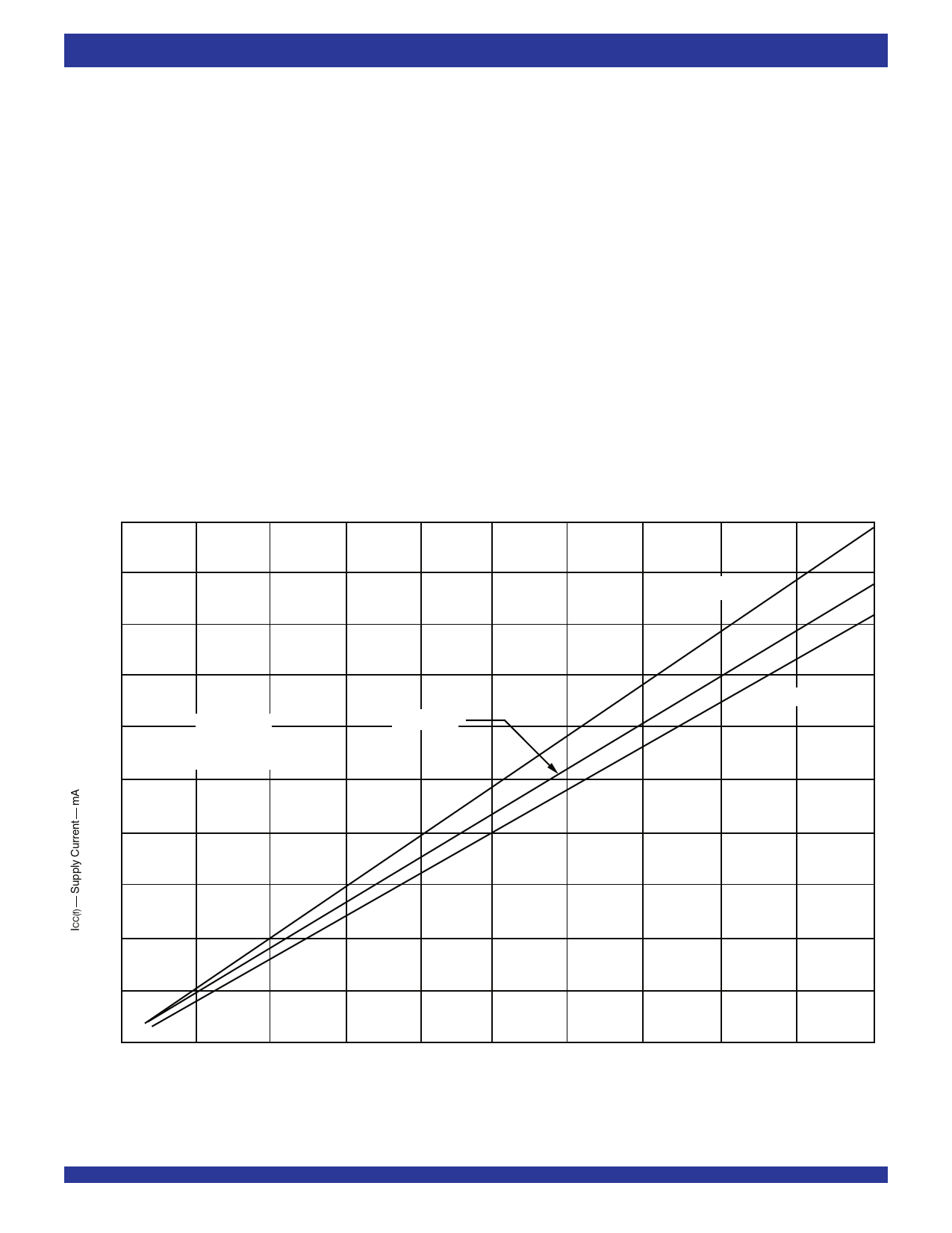
DETERMINING ACTIVE CURRENT CONSUMPTION AND POWER DISSIPATION
The ICC(f) current for the graph in Figure 1 was taken while simultaneously reading and writing a FIFO on the IDT72V3682/72V3692/72V36102 with
CLKA and CLKB set to fS. All data inputs and data outputs change state during each clock cycle to consume the highest supply current. Data outputs were
disconnected to normalize the graph to a zero capacitance load. Once the capacitance load per data-output channel and the number of these device's
inputs driven by TTL HIGH levels are known, the power dissipation can be calculated with the equation below.
CALCULATING POWER DISSIPATION
With ICC(f) taken from Figure 1, the maximum power dissipation (PT) of these FIFOs may be calculated by:
PT = VCC x ICC(f) + Σ(CL x VCC2 X fo)
N
where:
N
=
CL
=
fo
=
number of outputs = 36
output capacitance load
switching frequency of an output
100
90
80
70
60
50
40
30
20
10
0
0
fdata = 1/2 fS
TA = 25°C
CL = 0 pF
VCC = 3.3V
VCC = 3.6V
VCC = 3.0V
10
20
30
40
50
60
70
80
fS Clock Frequency MHz
Figure 1. Typical Characteristics: Supply Current (ICC) vs. Clock Frequency (fS)
7
90
100
4679 drw 04
Share Link: 