IDTVS330QG 데이터 시트보기 (PDF) - Integrated Device Technology
부품명
상세내역
제조사
IDTVS330QG Datasheet PDF : 10 Pages
| |||
IDTVS330
LOW ON-RESISTANCE WIDEBAND/VIDEO QUAD 2-CH
COMMERCIAL TEMPERATURE RANGE
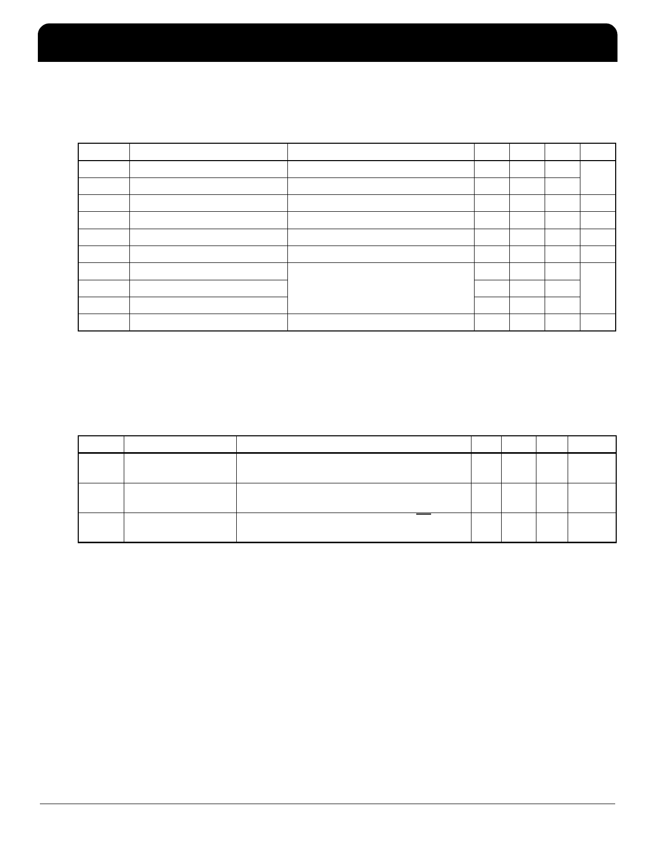
Dynamic Electrical Characteristics Over Operating Range
Following Conditions Apply Unless Otherwise Specified:
TA = 0°C to +70°C, VCC = 3.3V ± 5%.
Symbol
Parameter
Conditions
tON
Turn On Time
RL = 75Ω, CL = 20pF
tOFF
Turn Off Time
BW1
-3dB Bandwidth
RL = 75Ω, CL = 20pF
RL = 150Ω
XTALK Crosstalk
RIN = 10Ω, RL = 150Ω, 10MHz
DG
Differential Gain
RL = 150Ω, f = 3.58MHz
DP
CIN1
COFF1
CON1
Differential Phase
Input/Enable Capacitance
Capacitance, Switch Off
Capacitance, Switch On
RL = 150Ω, f = 3.58MHz
VIN = 0V, f = 1MHz
OIRR
Off Isolation
RL = 150Ω, 10MHz
1. This parameter is determined by device characterization but is not production tested.
Min.
—
—
—
—
—
—
—
—
—
—
Typ.
2.5
1.1
—
– 58
0.64
0.27
—
—
—
– 38
Max.
5
5
570
—
—
—
6
6
8
—
Unit
ns
MHz
dB
%
Deg.
pF
dB
Power Supply Characteristics
Symbol
Parameter
Conditions1
Min. Typ.2 Max. Unit
ICC
Quiescent Power
Supply Current
VCC = Max., IN = GND or VCC
— 0.1 3
µA
∆ICC
Power Supply Current
per Input @ TTL HIGH
VCC = Max., IN = 3.4V3
— — 2.5 mA
ICCD4
Supply Current per
Input per MHz
VCC = Max., S1, S2 and D Pins Open, EN = GND —
Control Input Toggling, 50%Duty Cycle
— 0.25 mA/MHz
1. For Max. or Min. conditions, use appropriate value specified under Electrical Characteristics for the applicable device.
2. Typical values are at VCC = 5.0V, +25°C ambient.
3. Per TTL driven input (VIN = 3.4V, control inputs only); S1, S2, and D pins do not contribute to ICC.
4. This current applies to the control inputs only and represent the current required to switch internal capacitance at the spec-
ified frequency. The S1, S2, and D I/O pins generate no significant AC or DC currents as they transition. This parameter
is not tested, but is guaranteed by design.
LOW ON-RESISTANCE WIDEBAND/VIDEO QUAD 2-CH
5
CONFIDENTIAL
IDTVS330
7012/6
Share Link: 