ILC6382-33 데이터 시트보기 (PDF) - Impala Linear Corporation
부품명
상세내역
제조사
ILC6382-33
Impala Linear Corporation

ILC6382-33 Datasheet PDF : 19 Pages
| |||
1-Cell to 3-Cell Boost with True Load Disconnect, 3.3V, 5V, or Adjustable Output
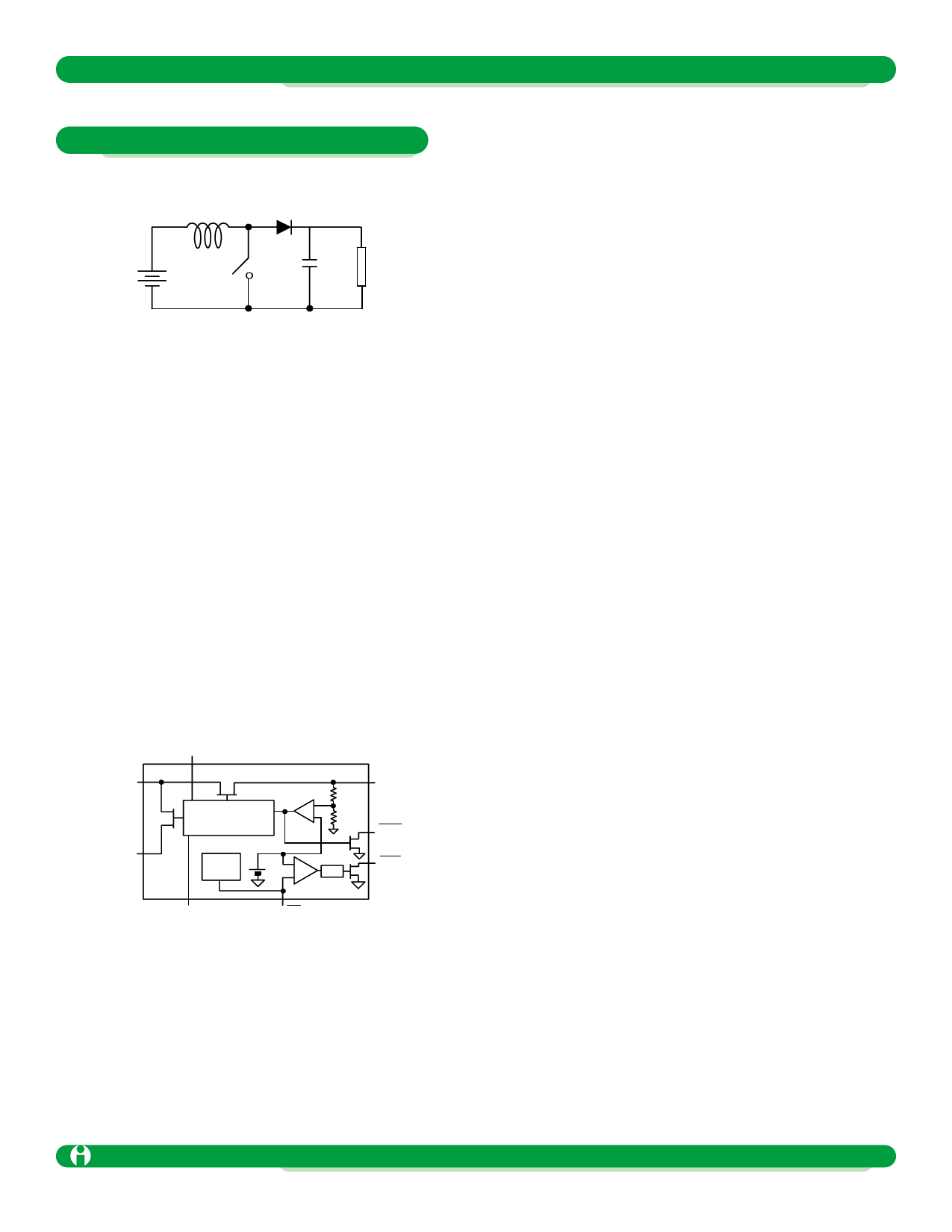
APPLICATIONS INFORMATION
The ILC6382 performs boost DC-DC conversion by control-
ling the switch element as shown in the simplified circuit in
figure 3 below.
Figure 3: Basic Boost Circuit
When the switch is closed, current is built up through the
inductor. When the switch opens, this current has to go
somewhere and is forced through the diode to the output.
As this on and off switching continues, the output capacitor
voltage builds up due to the charge it is storing from the
inductor current. In this way, the output voltage gets boost-
ed relative to the input.
In general, the switching characteristic is determined by the
output voltage desired and the current required by the load.
Specifically the energy transfer is determined by the power
stored in the coil during each switching cycle.
PL = ƒ(tON, VIN)
Synchronous Rectification
The ILC6382 also uses a technique called "synchronous
rectification" which removes the need for the external diode
used in other circuits. The diode is replaced with a second
switch or in the case of the ILC6382, an FET as shown in
figure 4 below.
VIN
LX
SW2
SW1
PWM/PFM
CONTROLLER
ILC6382
VOUT
-
+
POK
GND
SHUTDOWN
CONTROL
+
VREF
-
DELAY
LBO
SYNC
LB/SD
Figure 4: Simplified ILC6382 block diagram
The two switches now open and close in opposition to
eachother, directing the flow of current to either charge the
inductor or to feed the load. The ILC6382 monitors the volt-
age on the output capacitor to determine how much and
how often to drive the switches.
PWM Mode Operation
The ILC6382 uses a PWM or Pulse Width Modulation tech-
nique. The switches are constantly driven at typically
300kHz. The control circuitry varies the power being deliv-
ered to the load by varying the on-time, or duty cycle, of the
switch SW1 (see fig. 5). Since more on-time translates to
higher current build-up in the inductor, the maximum duty
cycle of the switch determines the maximum load current
that the device can support.
There are two key advantages of the PWM type controllers.
First, because the controller automatically varies the duty
cycle of the switch's on-time in response to changing load
conditions, the PWM controller will always have an opti-
mized waveform for a steady-state load. This translates to
very good efficiency at high currents and minimal ripple on
the output. Ripple is due to the output cap constantly
accepting and storing the charge received from the induc-
tor, and delivering charge as required by the load. The
"pumping" action of the switch produces a sawtooth-shaped
voltage as seen by the output.
The other key advantage of the PWM type controllers is that
the radiated noise due to the switching transients will
always occur at the (fixed) switching frequency. Many appli-
cations do not care much about switching noise, but certain
types of applications, especially communication equipment,
need to minimize the high frequency interference within
their system as much as possible. Using a boost converter
requires a certain amount of higher frequency noise to be
generated; using a PWM converter makes that noise high-
ly predictable thus easier to filter out.
PFM Mode Operation
There are downsides of PWM approaches, especially at
very low currents. Because the PWM technique relies on
constant switching and varying duty cycle to match the load
conditions, there is some point where the load current gets
too small to be handled efficiently. An actual switch con-
sumes some finite amount of current to switch on and off; at
very low currents this can be of the same magnitude as the
load current itself, driving switching efficiencies down to
50% and below. The ILC6382 overcomes this limitation by
automatically switching over to a PFM, or Pulse Frequency
Modulation, technique at low currents. This technique con-
serves power loss by only switching the output if the current
drain requires it. As shown in the figure 5, the waveform
actually skips pulses depending on the power needed by
the output. This technique is also called "pulse skipping"
because of this characteristic.
Impala Linear Corporation
ILC6382 1.5
(408) 574-3939 www.impalalinear.com
Oct 1999 6
Share Link: