INA3010N 데이터 시트보기 (PDF) - Unspecified
부품명
상세내역
제조사
INA3010N Datasheet PDF : 8 Pages
| |||
INA3010
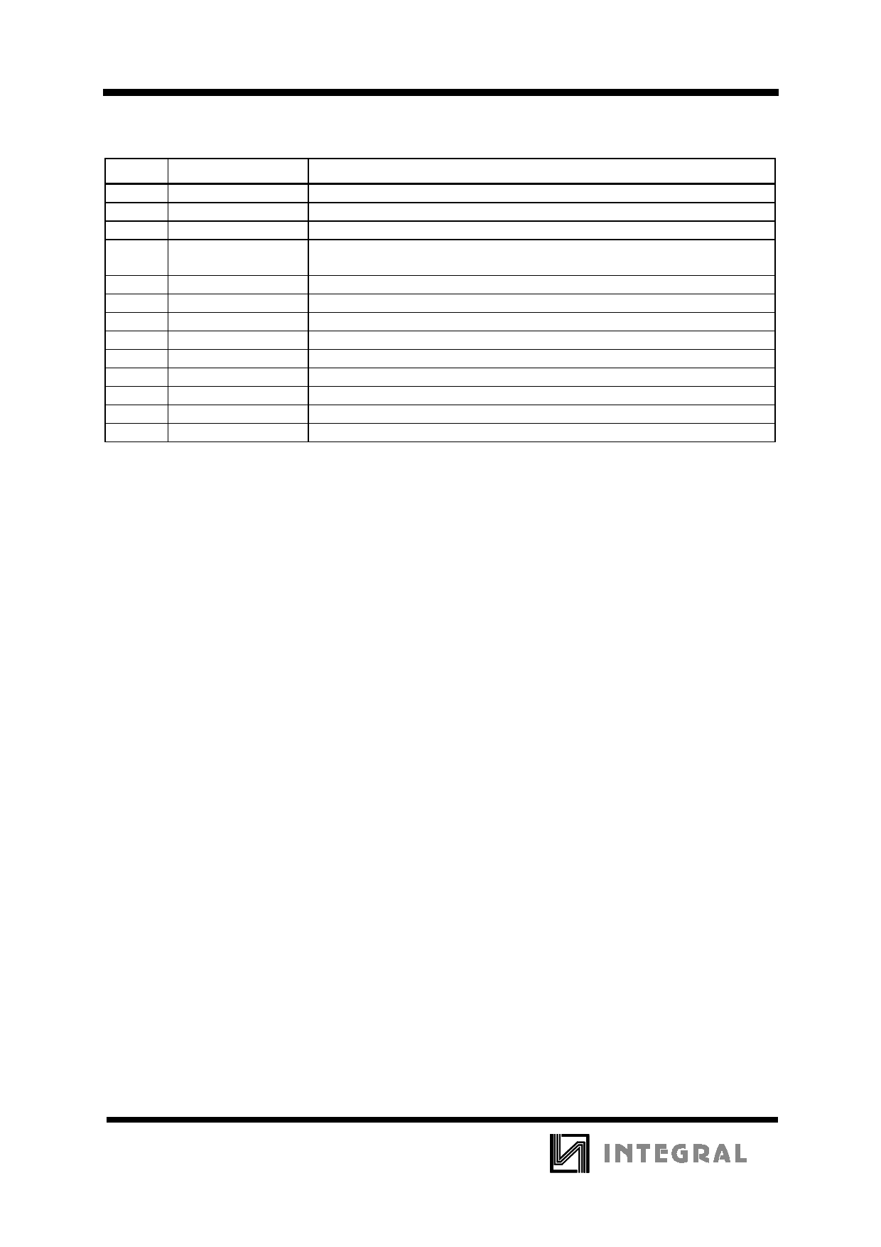
PIN DESCRIPTION
PIN No DESIGNATION
DESCRIPTION
1
X7 (IPU)
sense input from key matrix
2
SSM (I)
system mode selection input
3-6
Z0-Z3 (IPU)
sense inputs from key matrix
7
MDATA (OP3)
generated output data modulated with 1/2 the oscillator frequency at a 25%
duty factor
8
DATA (OP3)
generated output information
9-13 DR7-DR3 (ODN) scan drivers
14
GND
ground (0V)
15-17 DR2-DR0 (ODN) scan drivers
18
OSC (I)
oscillator input
19
TP2 (I)
test point 2
20
TP1 (I)
test point 1
21-27 X0-X6 (IPU)
sense inputs from key matrix
28
Vcc (I)
voltage supply
(I) = input
(IPU) = input with p-channel pull-up transistor
(ODN) = output with open drain n-channel transistor
(OP3) = output 3-state
FUNCTIONAL DESCRIPTION
Keyboard operation
Every connection of one X-input and one DR-output will be recognized as a legal key operation and will cause
the device to generate the corresponding code. The same applies to every connection of one Z-input to one DR-
output with the proviso that SSM must be LOW. When SSM is HIGH a wired connection must exist between a
Z-input and DR-output. If no connection is present the system number will not be generated. Activating two or
more X-inputs, Z-inputs or Z-inputs and X-inputs at the same time is an illegal action and inhibits further activity
(oscillator will not start).
When one X- or Z-input is connected to more than one DR-output, the last scan signal will be considered as
legal.
The maximum value of the contact series resistance of the switched keyboard is 7KΩ.
Inputs
In the quiescent state the command inputs X0 to X7 are held HIGH by an internal pull-up transistor. When the
system mode selection (SSM) input is LOW and the system is quiescent, the system inputs Z0 to Z3 are also held
HIGH by an internal pull-up transistor. When SSM is HIGH the pull-up transistor for the Z-inputs is switched
off, in order to prevent current flow, and a wired connection in the Z-DR matrix provides the system number.
Outputs
The output signal DATA transmits the generated information in accordance with the format illustrated by Fig.2
and Tables 1 and 2. The code is transmitted using a biphase technique as illustrated by Fig.3. The code consists
of four parts:
• Start part - 1.5 bits (2 x logic 1)
• Control part - 1 bit
• System part - 5 bits
• Command part - 6 bits
The output signal MDATA transmits the generated information modulated by 1/12 of the oscillator frequency
with a 50% duty factor.
In the quiescent state both DATA and MDATA are non-conducting (3-state outputs).
The scan driver outputs DR0 to DR7 are open drain n-channel transistors and conduct when the circuit is
quiescent. After a legal key operation the scanning cycle is started and the outputs switched to the conductive
state one by one. The DR-outputs were switched off at the end of the preceding debounce cycle.
2
Share Link: 