INA3010N 데이터 시트보기 (PDF) - Integral Corp.
부품명
상세내역
제조사
INA3010N Datasheet PDF : 8 Pages
| |||
INA3010
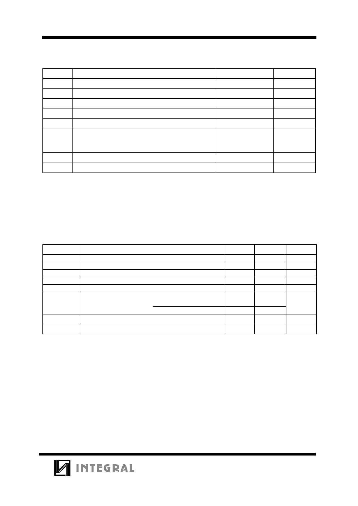
MAXIMUM RATINGS*
Symbol
VCC
VIN
VOUT
IIN
IOUT
PDO
PDO
PD
Tstg
Parameter
DC Supply Voltage (Referenced to GND)
DC Input Voltage (Referenced to GND)*
DC Output Voltage (Referenced to GND)*
DC Input Current
DC Output Current
Maximum Power Dissipation
OSC output
other outputs
Power Dissipation in Still Air
Storage Temperature
Value
Unit
-0.5 to +8.5
V
-0.5 to VCC +0.5
V
-0.5 to VCC +0.5
V
±10
mA
±10
mA
50
mW
100
mW
200
mW
-65 to +150
°C
*VCC + 0.5 must not exceeed 9.0V..
*Maximum Ratings are those values beyond which damage to the device may occur.
Functional operation should be restricted to the Recommended Operating Conditions.
+Derating - Plastic DIP: - 10 mW/°C from 65° to 85°C
SOIC Package: : - 7 mW/°C from 65° to 85°C
RECOMMENDED OPERATING CONDITIONS
Symbol
VCC
VIH
VIL
VOUT
IIN
IOL
IOH
TA
Parameter
DC Supply voltage (Reference to GND)
DC Input voltage (HIGH)
DC Input voltage (LOW)
DC Output Voltage (MDATA, DATA)
DC Input Current
DC Output Current (LOW)
pins 7,8
pins 9-13; 15-17
DC Output Current (MDATA, DATA)
Operating Temperature, All Package Types
Min
Max
Unit
2.0
7.0
V
0.7VCC
VCC
V
0
0.3VCC
V
-
7.0
V
-
±10
mA
-
0.6
mA
0.3
-
-0.4
mA
-25
85
oC
This device contains protection circuitry to guard against damage due to high static voltages or electric
fields. However, precautions must be taken to avoid applications of any voltage higher than maximum rated
voltages to this high-impedance circuit. For proper operation, VIN and VOUT should be constrained to the range
GND≤(VIN or VOUT)≤VCC.
Unused inputs must always be tied to an appropriate logic voltage level (e.g., either GND or VCC).
Unused outputs must be left open.
5
Share Link: 