IS25F011A 데이터 시트보기 (PDF) - Integrated Silicon Solution
부품명
상세내역
제조사
IS25F011A
Integrated Silicon Solution

IS25F011A Datasheet PDF : 23 Pages
| |||
IS25F011A
IS25F021A
IS25F041A
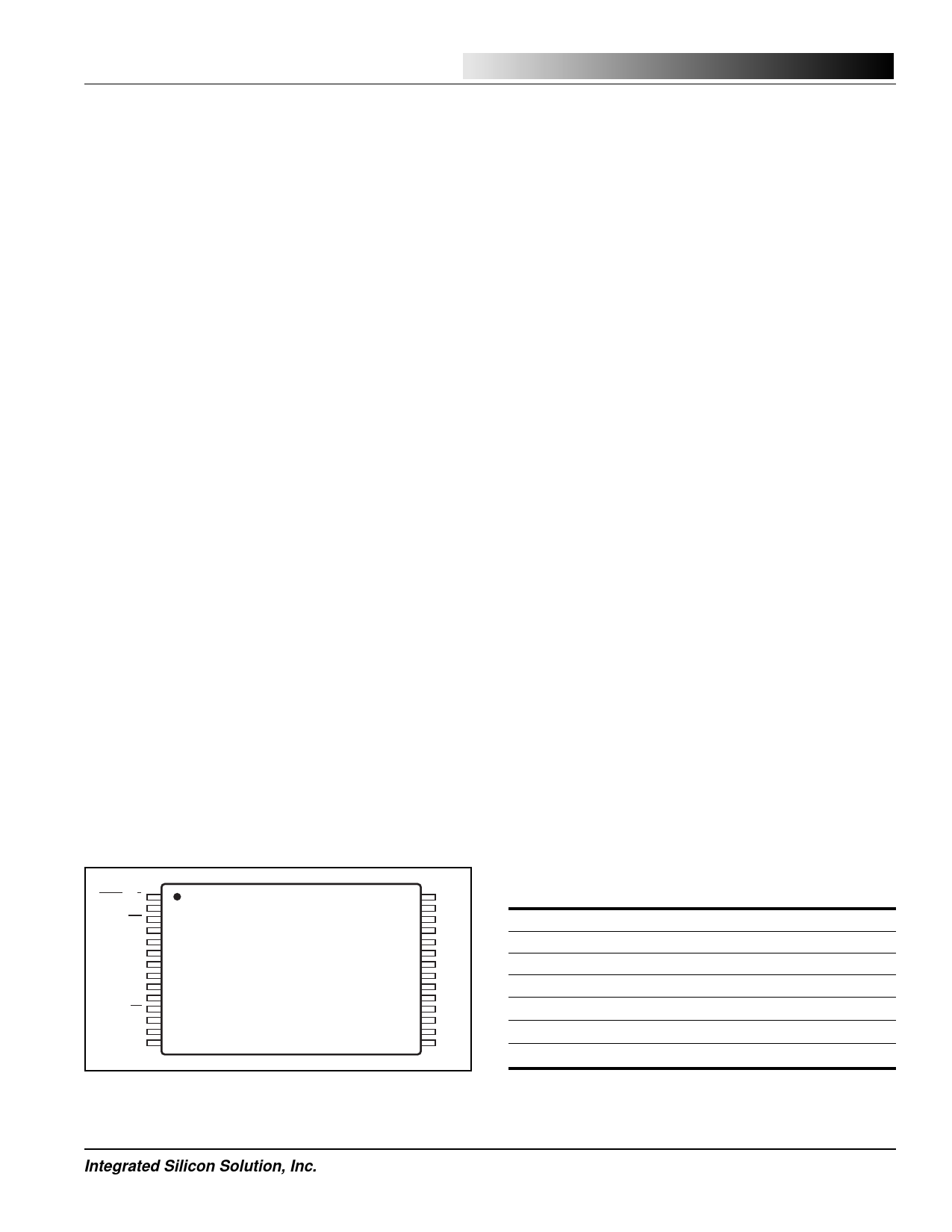
Pin Descriptions
Package
The IS25F011A, IS25F021A, and IS25F041A are
available in a 28-pin TSOP (Type I) surface mount
package. See Figure 3 and Table 1 for pin assign-
ments. All interface and supply pins are on one
side of the package. The “No Connect” (NC) pins
are not connected to the device, allowing the pads
and the area around them to be used for routing PCB
system traces. The devices are also available in a
cost-effective and space-efficient removable Serial
Flash Module package.
Serial Data Imput (SI)
The SPI bus Serial Data Input (SI) provides a means
for data to be written to (shifted into) the device.
Serial Data Output (SO)
The SPI bus Serial Data Output (SO) provides a
means for data to be read from (shifted out of) the
device during a read operation. When the device is
deselected (CS=1 or HOLD=0) the SO pin is in a
high-impedance state.
Serial Clock (SCK)
All commands and data written to the Serial Input
(SI) are clocked relative to the rising edge of the
Serial Clock (SCK). All data read from the Serial
Data Output (SO) is clocked relative to the falling or
rising edge of SCK as specified in the nonvolatile
configuration register. The data output clock edge is
factory-programmed to the default condition of the
falling edge, allowing compatibility with standard
SPI systems. Clock rates of up to 16 MHz for 5V
devices and up to 8 MHz for 3V devices are sup-
ported.
ISSI ®
Chip Select (CS)
1 The IS25F011A, IS25F021A, and IS25F041A are se-
lected for operation when the Chip Select input (CS) is
asserted low. Upon power-up, an initial low-to-high transi-
tion of CS is required before any command sequence will
be acknowledged. The device can be deselected to a non-
2 active state when CS is brought high. Once deselected,
the SO pin will enter a high-impedance state and power
consumption will decrease to standby levels unless pro-
gramming is in process, in which case standby will resume
when programming is complete.
3
Write Protect (WP)
The Write Protect input (WP) works in conjunction with the
4 write protect range set in the configuration register bits.
When WP is asserted (active low) the entire Flash memory
array is write protected. When high, any Flash memory
sector can be written to unless its address is within the
write protect range that is set in the configuration register.
5
Hold or Ready/Busy (HOLD or R/B)
This multi-function pin can serve either as a Hold input
(HOLD) or as a Ready-Busy output (R/B). The pin function
6 is user-programmable via the nonvolatile configuration
register. Factory-programmed as a no-connect, the pin
can be reconfigured as a Ready-Busy output or as a Hold
input by setting the configuration register. See the configu-
7 ration register section of this data sheet for further details.
Power Supply Pins (Vcc and GND)
The IS25F011A, IS25F021A, and IS25F041A support
8 single power supply Read and Erase/Write operations in
5V (4.5V -5.5V) and 3V (2.7V-3.6V) Vcc versions. Typical
active power is as low as 5 mA for the 3V version with
standby current less than 1 µA.
9
HOLD-R/B 1
NC 2
WP 3
NC 4
NC 5
VCC 6
GND 7
NC 8
NC 9
NC 10
CS 11
SCK 12
SI 13
SO 14
28
NC
27
NC
26
NC
25
NC
24
NC
23
NC
22
NC
21
NC
20
NC
19
NC
18
NC
17
NC
16
NC
15
NC
Figure 3. IS25F011A, IS25F021A, and IS25F041A
Pin Assignments, 28-Pin TSOP (Type I)
Integrated Silicon Solution, Inc.
PRELIMINARY SF001-1A
06/24/98
Table 1. Pin Descriptions
10
SI
SO
SCK
CS
WP
, Hold R/B
Vcc
Serial Data Input
Serial Data Output
Serial Clock Input
11
Chip Select Input
Write Protect Input
12 Hold Input or Read Busy Output
Power Supply
3
Share Link: