IS25F011A 데이터 시트보기 (PDF) - Integrated Silicon Solution
부품명
상세내역
제조사
IS25F011A
Integrated Silicon Solution

IS25F011A Datasheet PDF : 23 Pages
| |||
IS25F011A
IS25F021A
IS25F041A
register, the configuration register will maintain its setting
even when power is removed. The factory default setting
for bits CF8-CF0 is: 0 0000 1001 B(write protect range =
none, read uses falling edge of the clock, and pin 1 = no
connect). Bits CF15-CF9 are reserved. When writting to
the configuration register CF15-CF9 should be 0. When
reading, the settings of CF15-CF9 should be ignored.
Standard write endurance rating of the memory array
allows for 10,000 erase/write cycles. Extended endur-
ance to 100,000 cycles is possible using ECC techniques
like those provided in the SFK-SPI Development Kit (see
High Data Integrity Application, page 19). The rating of the
configuration register EEPROM cells, however, is 1,000
write cycles. This is more than adequate considering the
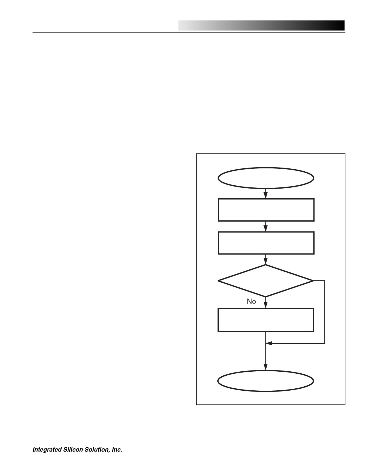
configuration seldom needs to be changed. To minimize
writes to the configuration register, the configuration
register should be read upon power-up to determine if a
change is required. If no change is needed, the write
configuration command can be skipped. This process will
extend the life of the configuration register and save
processing time (Figure 7).
Alternate Oscillator Frequency, AF
Flash memory devices have charge pump oscillators to
generate internal high-voltages used for programming
nonvolatile memory cells. In some applications, the oscil-
lator frequency of the charge pump may cause noise
interference. To solve this problem, an alternate oscilla-
tor frequency (AF) can be selected by setting bit CF[8]
of the configuration register. The alternate frequency is
a non-harmonic frequency of the standard oscillator. The
factory default setting is for the standard oscillator fre-
quency, AF equal to 0.
AF=0 Standard Oscillator Frequency is used.
AF=1 Alternate Oscillator Frequency is used.
Write Protect Range and Direction, WR[3:0], WD
The write protect range and direction bits WR[3:0] and
WD are located at configuration bits CF[7:4] and CF[3]
respectively. The write protect range and direction bits
select how the array is protected. They work in conjunc-
tion with the WP input pin, valid only if WP is inactive
(high). WR[3:0] can select write protection of all sectors,
none of the sectors, or specific sectors grouped in blocks
of 32 (~8 KB). The WD bit specifies whether the protected
block range starts from the first sector, address 0 (000H),
or from the last sector (1FFH for the IS25F011A, 3FFH for
the IS25F021A, and 7FF for the IS25F041A). Table 2 lists
the write protect sector range for both devices. Once
protected, all further writes to sectors within the range will
be ignored . The factory default setting is with no write
protected sectors, WR=[0,0,0,0] and WD=1.
ISSI ®
Read Clock Edge, RCE
The Read Clock Edge bit (RCE) is located at configura-
tion bit location CF[2]. It selects which edge of the clock
1 (SCK) is used while reading data out of the device.
Although the SPI protocol specifies that data is written
during the rising edge and read on the falling edge of the
clock, if required, the output can be driven on the rising
edge of the clock by setting the configuration registers
2 RCE bit to a 1. Using the rising edge of clock for data
reads may be beneficial to the timing of some high-speed
systems. The factory default setting is the falling edge of
SCK.
3
RCE=0 Read data is output on the falling edge of SCK.
RCE=1 Read data is output on the rising edge of SCK.
4
System Power-up
5
Read Device Information Sector,
Verify Device Density and Type
6
Read Configuration Register
Verify bits are Set as Needed
7
Configuration
Yes
Setting is Correct?
8
No
Write Configuration Register
9
to Correct Setting
10
11
Application Routines
12
Figure 7. Flow Chart for Checking the Configuration
Register upon Power-up
Integrated Silicon Solution, Inc.
7
PRELIMINARY SF001-1A
06/24/98
Share Link: