CA5160(2003) 데이터 시트보기 (PDF) - Intersil
부품명
상세내역
제조사
CA5160
(Rev.:2003)
(Rev.:2003)
Intersil

CA5160 Datasheet PDF : 19 Pages
| |||
CA5160
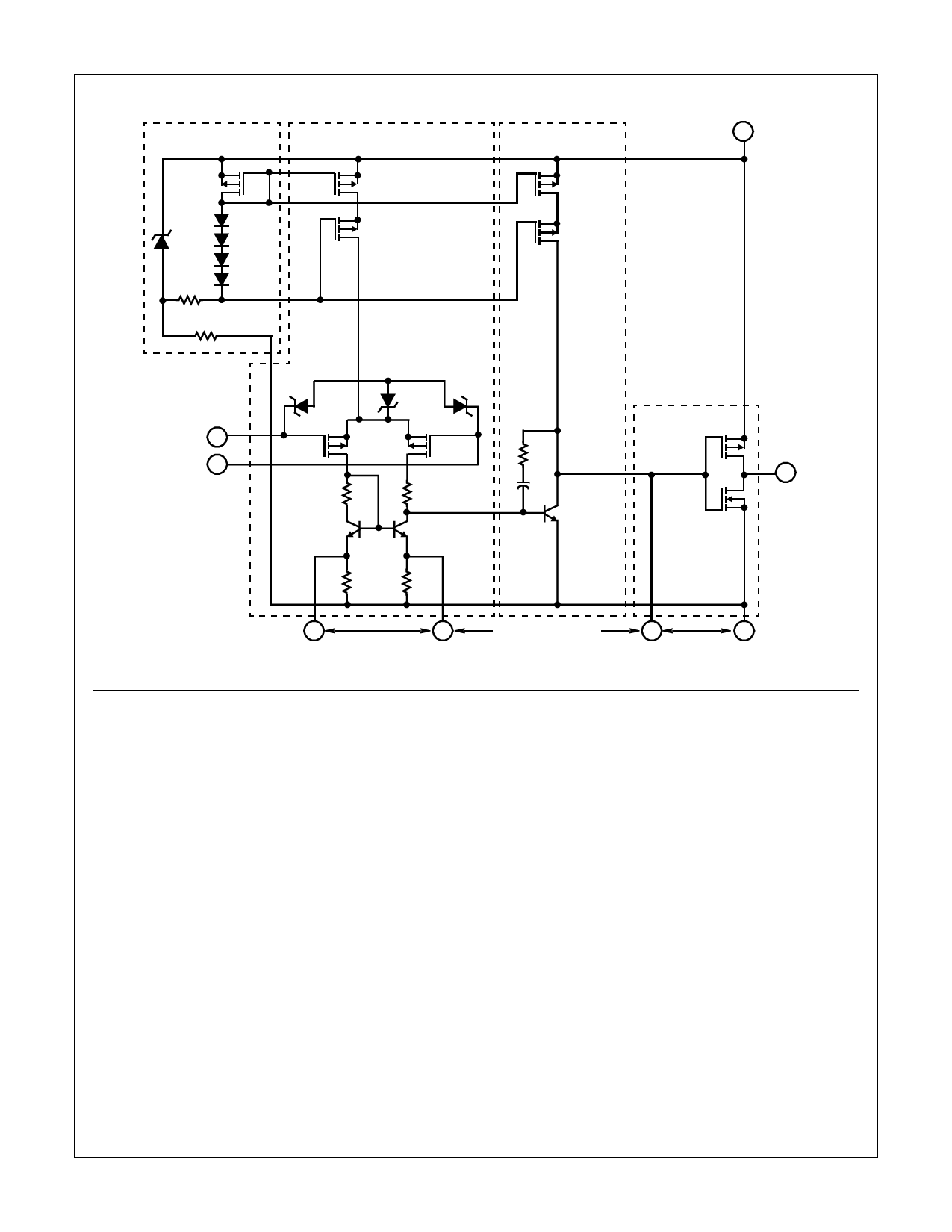
Schematic Diagram
BIAS CIRCUIT
CURRENT SOURCE
FOR Q6 AND Q7
Q1
Q2
D1
Q4
Z1
D2
8.3V
D3
R1
40kΩ
D4
R2
5kΩ
NON-INV.
INPUT
3+
2
-
INV. INPUT
INPUT STAGE
D5
D6
D7
Q6 Q7
R3
1kΩ
Q9
R4
1kΩ
Q10
“CURRENT SOURCE
LOAD” FOR Q11
Q3
Q5
7 V+
SECOND
STAGE
2kΩ
30
pF
Q11
OUTPUT
STAGE
Q8
OUTPUT
6
Q12
R5
R6
1kΩ
1kΩ
5
1
OFFSET NULL
SUPPLEMENTARY
COMP IF DESIRED
NOTE: Diodes D5 through D7 provide gate oxide protection for MOSFET Input Stage.
8
4
STROBING
Application Information
Circuit Description
Refer to the block diagram of the CA5160 CMOS
Operational Amplifier. The input terminals may be operated
down to 0.5V below the negative supply rail, and the output
can be swung very close to either supply rail in many
applications. Consequently, the CA5160 circuit is ideal for
single supply operation. Three class A amplifier stages,
having the individual gain capability and current
consumption shown in the block diagram, provide the total
gain of the CA5160. A biasing circuit provides two potentials
for common use in the first and second stages. Terminals 8
and 1 can be used to supplement the internal phase
compensation network if additional phase compensation or
frequency roll-off is desired. Terminals 8 and 4 can also be
used to strobe the output stage into a low quiescent current
state. When Terminal 8 is tied to the negative supply rail
(Terminal 4) by mechanical or electrical means, the output
potential at Terminal 6 essentially rises to the positive supply
rail potential at Terminal 7. This condition of essentially zero
current drain in the output stage under the strobed “OFF”
condition can only be achieved when the ohmic load
resistance presented to the amplifier is very high (e.g., when
the amplifier output is used to drive CMOS digital circuits in
comparator applications).
Input Stages
The circuit of the CA5160 is shown in the schematic diagram.
It consists of a differential input stage using PMOS field effect
transistors (Q6, Q7) working into a mirror pair of bipolar
transistors (Q9, Q10) functioning as load resistors together
with resistors R3 through R6. The mirror pair transistors also
function as a differential-to-single-ended converter to provide
base drive to the second-stage bipolar transistor (Q11). Offset
nulling, when desired, can be effected by connecting a
100,000Ω potentiometer across Terminals 1 and 5 and the
potentiometer slider arm to Terminal 4.
Cascode-connected PMOS transistors Q2, Q4, are the
constant current source for the input stage. The biasing
circuit for the constant current source is subsequently
described. The small diodes D5 through D7 provide gate-
oxide protection against high voltage transients, including
static electricity during handling for Q6 and Q7.
5
Share Link: