ISL59448 데이터 시트보기 (PDF) - Intersil
부품명
상세내역
제조사
ISL59448 Datasheet PDF : 14 Pages
| |||
ISL59448
AC Test Circuits
VIN
50Ω
or
75Ω
ISL59448
LCRIT
*CL
1.1pF
RL
500Ω, or
150Ω
VOUT
*CL Includes PCB trace capacitance
FIGURE 27A. TEST CIRCUIT WITH OPTIMAL OUTPUT LOAD
ISL59448
LCRIT
VIN
50Ω
or
75Ω
CL RS
CS
RL
500Ω, or
75Ω
FIGURE 27B. INTER-STAGE APPLICATION CIRCUIT
VIN
50Ω
ISL59448
LCRIT
RS
475Ω
*CL
1.1pF
56.2Ω
TEST
EQUIPMENT
50Ω
*CL Includes PCB trace capacitance
FIGURE 27C. 500Ω TEST CIRCUIT WITH 50Ω LOAD
VIN
50Ω,or
75Ω
ISL59448
LCRIT
RS
*CL 118Ω
1.1pF
86.6Ω
TEST
EQUIPMENT
50Ω
*CL Includes PCB trace capacitance
FIGURE 27D. 150Ω TEST CIRCUIT WITH 50Ω LOAD
VIN
50Ω
or
75Ω
ISL59448
LCRIT
RS
*CL 50Ω or 75Ω
1.1pF
TEST
EQUIPMENT
50Ω or 75Ω
*CL Includes PCB trace capacitance
FIGURE 27E. BACKLOADED TEST CIRCUIT FOR 75Ω VIDEO
CABLE APPLICATION
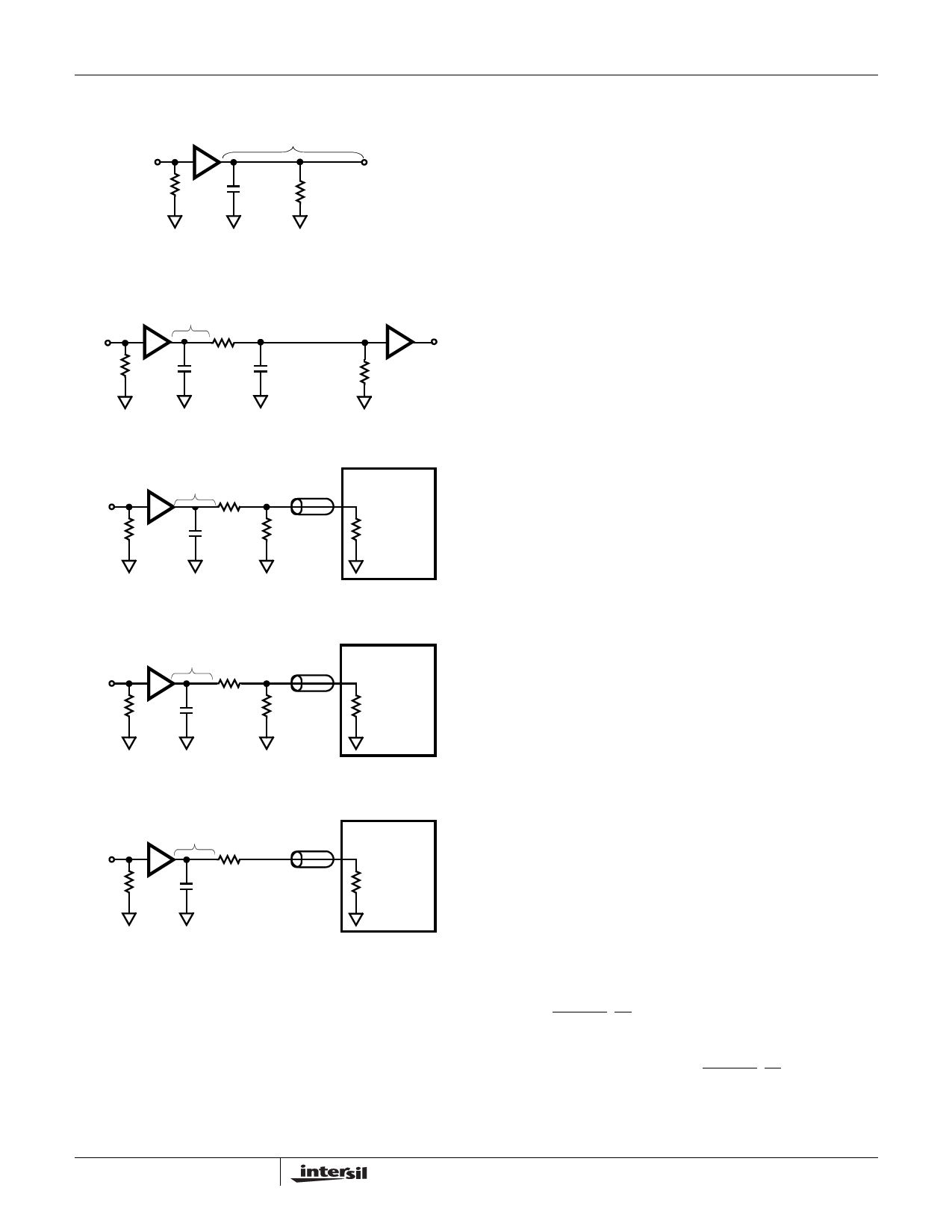
AC Test Circuits
Figure 27C and 27D illustrate the optimum output load for
testing AC performance at 500Ω and 150Ω loads. Figure
27E illustrates the optimun output load for 50Ω and 75Ω
cable-driving.
Application Information
General
Key features of the ISL59448 include a fixed gain of 2,
buffered high impedance analog inputs and excellent AC
performance at output loads down to 150Ω for video cable-
driving. The current feedback output amplifiers are stable
operating into capacitive loads.
For the best isolation and crosstalk rejection, all GND pins
and NIC pins must connect to the GND plane.
AC Design Considerations
High speed current-feed amplifiers are sensitive to
capacitance at the inverting input and output terminals. The
ISL59448 has an internally set gain of 2, so the inverting
input is not accessible. Capacitance at the output terminal
increases gain peaking (Figure 1) and pulse overshoot
(Figures15 thru 18). The AC response of the ISL59448 is
optimized for a total capacitance of 1.1pF over the load
range of 150Ω to 500Ω.
PC board trace length should be kept to a minimum in order
to minimize output capacitance and prevent the need for
controlled impedance lines. At 500MHz trace lengths
approaching 1” begin exhibiting transmission line behavior
and may cause excessive ringing if controlled impedance
traces are not used. Figure 27A shows the optimum inter-
stage circuit when the total output trace length is less than
the critical length of the highest signal frequency.
For applications where pulse response is critical and where
inter-stage distances exceed LCRIT, the circuit shown in
Figure 27B is recommended. Resistor RS constrains the
capacitance seen by the amplifier output to the trace
capacitance from the output pin to the resistor. Therefore,
RS should be placed as close to the ISL59448 output pin as
possible. For inter-stage distances much greater than LCRIT,
the back-loaded circuit shown in Figure 27E should be used
with controlled impedance PCB lines, with RS and RL equal
to the controlled impedance.
For applications where inter-stage distances are long, but
pulse response is not critical, capacitor CS can be added to
low values of RS to form a low-pass filter to dampen pulse
overshoot. This approach avoids the need for the large gain
correction required by the -6dB attenuation of the back-
loaded controlled impedance interconnect. Load resistor RL
is still required but can be 500Ω or greater, resulting in a
much smaller attenuation factor.
Control Signals
S0, S1, ENABLE, LE, HIZ - These are binary coded,
TTL/CMOS compatible control inputs. The S0, S1 pins select
the inputs. All three amplifiers are switched simultaneously
from their respective inputs. The ENABLE, LE, HIZ pins are
used to disable the part to save power, latch in the last logic
state and three-state the output amplifiers, respectively. For
11
FN6160.2
March 29, 2006
Share Link: 