ISL8088 데이터 시트보기 (PDF) - Intersil
부품명
상세내역
제조사
ISL8088 Datasheet PDF : 18 Pages
| |||
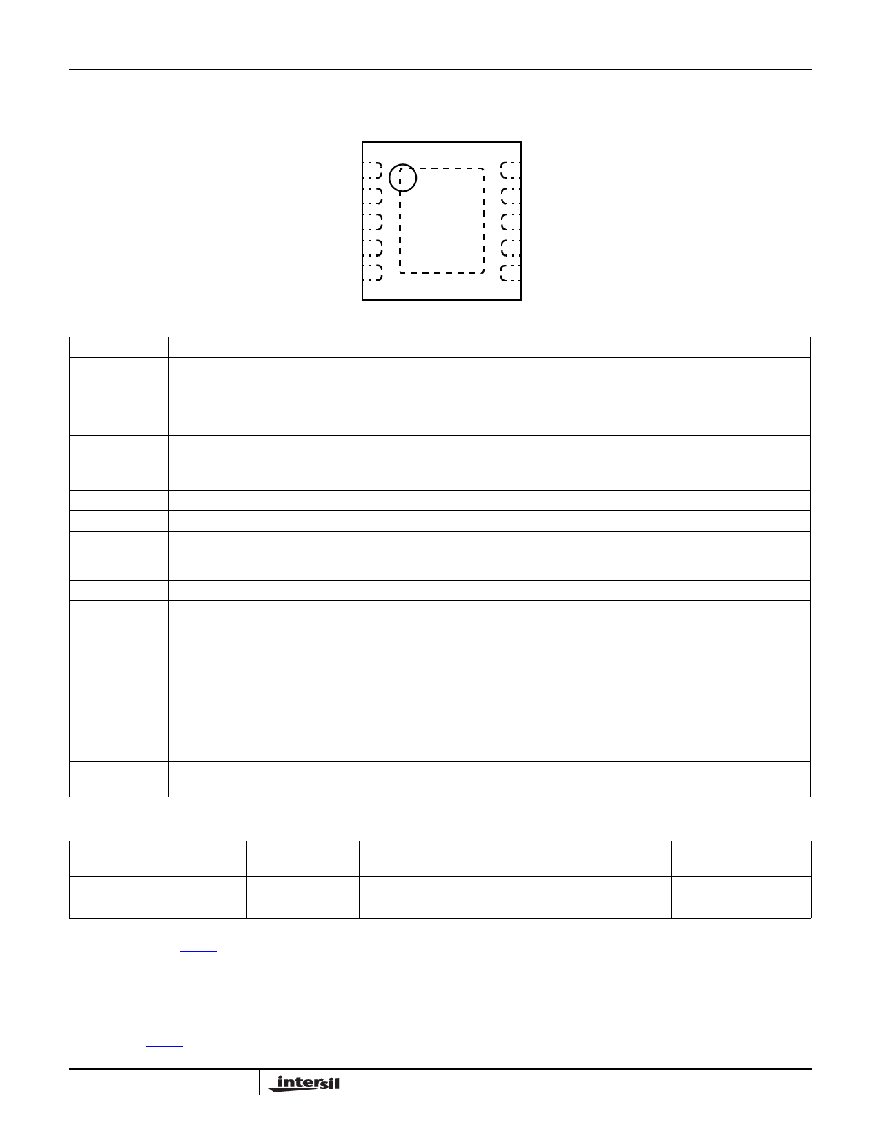
Pin Configuration
ISL8088
ISL8088
(10 LD 3X3 DFN)
TOP VIEW
FB1 1
EN1 2
VIN 3
LX1 4
NC 5
10 FB2
9 EN2
PD
8 PG
7 LX2
6 SYNC
Pin Descriptions
DFN SYMBOL
DESCRIPTION
1
FB1 The feedback network of the Channel 1 regulator. FB1 is the negative input to the transconductance error
amplifier. The output voltage is set by an external resistor divider connected to FB1. With a properly selected
divider, the output voltage can be set to any voltage between the power rail (reduced by converter losses) and
the 0.6V reference. There is an internal compensation to meet a typical application. In addition, the regulator
power-good and undervoltage protection circuitry use FB1 to monitor the Channel 1 regulator output voltage.
2
EN1 Regulator Channel 1 enable pin. Enable the output, VOUT1, when driven to high. Shutdown the VOUT1 and
discharge output capacitor when driven to low. Do not leave this pin floating.
3
VIN Input supply voltage. Connect 10µF ceramic capacitor to power ground.
4
LX1 Switching node connection for Channel 1. Connect to one terminal of inductor for VOUT1.
5
NC Recommended to connect this pin to the exposed pad.
6
SYNC Mode Selection pin. Connect to logic high or input voltage VIN for PFM mode; connect to logic low or ground
for forced PWM mode. Connect to an external function generator for Synchronization, and negative edge
trigger. Do not leave this pin floating.
7
LX2 Switching node connection for Channel 2. Connect to one terminal of inductor for VOUT2.
8
PG 1ms timer output. At power-up or EN_ HI, this output is a 1ms delayed Power-Good signal for both the VOUT1
and VOUT2 voltages. There is an internal 1MΩ pull-up resistor.
9
EN2 Regulator Channel 2 enable pin. Enable the output, VOUT2, when driven to high. Shutdown the VOUT2 and
discharge output capacitor when driven to low. Do not leave this pin floating.
10
FB2 The feedback network of the Channel 2 regulator. FB2 is the negative input to the transconductance error
amplifier. The output voltage is set by an external resistor divider connected to FB2. With a properly selected
divider, the output voltage can be set to any voltage between the power-rail (reduced by converter losses) and
the 0.6V reference. There is an internal compensation to meet a typical application.
In addition, the regulator power-good and undervoltage protection circuitry use FB2 to monitor the Channel 2
regulator output voltage.
-
PD The exposed pad must be connected to PGND for proper electrical performance. Add as much vias as possible
for optimal thermal performance.
Ordering Information
PART NUMBER
(Notes 2, 3)
PART
MARKING
TEMP. RANGE
(°C)
PACKAGE
(Pb-Free)
PKG.
DWG. #
ISL8088IRZ
8088
-40 to +85
10 Ld 3x3 DFN
L10.3x3C
ISL8088IRZ-T (Note 1)
8088
-40 to +85
10 Ld 3x3 DFN
L10.3x3C
NOTES:
1. Please refer to TB347 for details on reel specifications.
2. These Intersil Pb-free plastic packaged products employ special Pb-free material sets, molding compounds/die attach
materials, and 100% matte tin plate plus anneal (e3 termination finish, which is RoHS compliant and compatible with both
SnPb and Pb-free soldering operations). Intersil Pb-free products are MSL classified at Pb-free peak reflow temperatures that
meet or exceed the Pb-free requirements of IPC/JEDEC J STD-020.
3. For Moisture Sensitivity Level (MSL), please see device information page for ISL8088. For more information on MSL please see
techbrief TB363.
3
FN6858.1
April 29, 2010
Share Link: 