IXDD415 데이터 시트보기 (PDF) - IXYS CORPORATION
부품명
상세내역
제조사
IXDD415 Datasheet PDF : 8 Pages
| |||
IXDD415SI
APPLICATIONS INFORMATION
High Frequency Gate Drive Circuit
The circuit diagram in figure 14 is a circuit diagram for a
very high switching speed, high frequency gate driver
circuit using the IXDD415SI. This is the circuit used in
the EVDD415 Evaluation Board,and is capable of driving
a MOSFET at up to the maximum operating limits of the
IXDD415. The circuit's very high switching speed and
high frequency operation dictates the close attention to
several important issues with respect to circuit design.
The three key elements are circuit loop inductance, Vcc
bypassing and grounding.
Circuit Loop Inductance
Referring to Figure 14, the Vcc to Vcc ground current
path defines the loop which will generate the inductive
term. This loop must be kept as short as possible. The
output leads (pins 24, 23, 22, 21, 20, and 19) must be
no further than 0.375 inches (9.5mm) from the gate of
the MOSFET. Furthermore the output ground leads (pins
25, 26, 27 and 28 on one end of the IC and pins 15, 16,
17, and 18 on the other end of the IC) must provide a
balanced symmetric coplanar ground return for optimum
operation.
Vcc Bypassing
In order for the circuit to turn the MOSFET on properly,
the IXDD415 must be able to draw up to 15A of current
per output channel from the Vcc power supply in 2-6ns
(depending upon the input capacitance of the MOSFET
being driven). This means that there must be very low
impedance between the driver and the power supply.
The most common method of achieving this low
impedance is to bypass the power supply at the driver
with a capacitance value that is at least two orders of
magnitude larger than the load capacitance. Usually,
this is achieved by placing two or three different types of
bypassing capacitors, with complementary impedance
curves, very close to the driver itself. (These capacitors
should be carefully selected, low inductance, low
resistance, high-pulse current-service capacitors). Care
should be taken to keep the lengths of the leads
between these bypass capacitors and the IXDD415 to an
absolute minimum.
The bypassing should be comprised of several values of
chip capacitors symmetrically placed on ether side of
the IC. Recommended values are .01uF, .47uF chips
and at least two 4.7uF tantalums.
Grounding
In order for the design to turn the load off properly, the
IXDD415 must be able to drain this 15A of current into an
adequate grounding system. There are three paths for
returning current that need to be considered: Path #1 is
between the IXDD415 and its load. Path #2 is between the
IXDD415 and its power supply. Path #3 is between the
IXDD415 and whatever logic is driving it. All three of these
paths should be as low in resistance and inductance as
possible, and thus as short as practical.
Output Lead Inductance
Of equal importance to supply bypassing and grounding are
issues related to the output lead inductance. Every effort
should be made to keep the leads between the driver and
its load as short and wide as possible, and treated as
coplanar transmission lines.
In configurations where the optimum configuration of circuit
layout and bypassing cannot be used, a series resistance
of a few Ohms in the gate lead may be necessary to prevent
ringing.
Heat Sinking
For high power operation, the bottom side metalized heat
sink pad should be epoxied to the circuit board ground
plane, or attached to an appropriate heat sink, using
thermally conductive epoxy. The heat sink tab is connected
to ground.
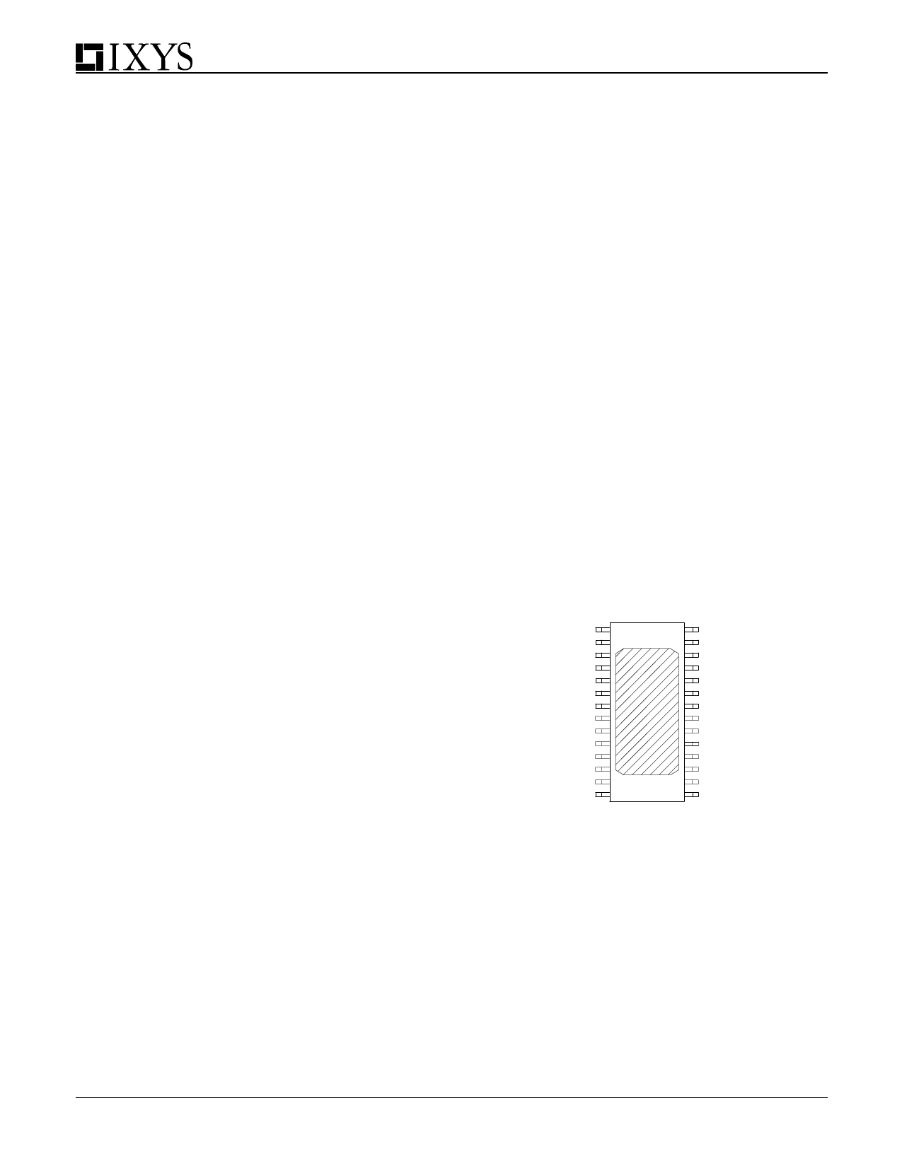
Figure 15: IXDD415SI Bottom Side
Heat Sinking Metalization
7
Share Link: 