IXDD415 데이터 시트보기 (PDF) - IXYS CORPORATION
부품명
상세내역
제조사
IXDD415 Datasheet PDF : 8 Pages
| |||
IXDD415SI
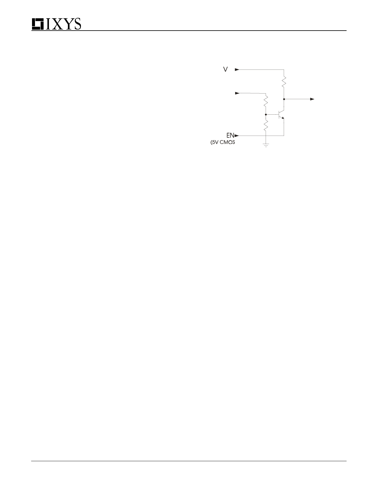
TTL to High Voltage CMOS Level Translation
The enable (EN) input to the IXDD415 is a high voltage
CMOS logic level input where the EN input threshold is ½ V ,
CC
and may not be compatible with 5V CMOS or TTL input levels.
The IXDD415 EN input was intentionally designed for
enhanced noise immunity with the high voltage CMOS logic
levels. In a typical gate driver application, VCC =15V and the
EN input threshold at 7.5V, a 5V CMOS logical high input
applied to this typical IXDD415 application’s EN input will be
misinterpreted as a logical low, and may cause undesirable
or unexpected results. The note below is for optional
adaptation of TTL or 5V CMOS levels.
The circuit in Figure 16 alleviates this potential logic level
misinterpretation by translating a TTL or 5V CMOS logic input
to high voltage CMOS logic levels needed by the IXDD415 EN
input. From the figure, VCC is the gate driver power supply,
typically set between 8V to 20V, and VDD is the logic power
supply, typically between 3.3V to 5.5V. Resistors R1 and R2
form a voltage divider network so that the Q1 base is posi-
tioned at the midpoint of the expected TTL logic transition
levels.
A TTL or 5V CMOS logic low, VTTLLOW=~<0.8V, input applied to
the Q1 emitter will drive it on. This causes the level translator
output, the Q1 collector output to settle to VCESATQ1 +
V =<~2V, which is sufficiently low to be correctly
TTLLOW
interpreted as a high voltage CMOS logic low (<1/3VCC=5V for
V =15V given in the IXDD415 data sheet.)
CC
A TTL high, VTTLHIGH=>~2.4V, or a 5V CMOS high,
V5VCMOSHIGH=~>3.5V, applied to the EN input of the circuit in
Figure 16 will cause Q1 to be biased off. This results in Q1
collector being pulled up by R3 to VCC=15V, and provides a
high voltage CMOS logic high output. The high voltage CMOS
logical EN output applied to the IXDD415 EN input will enable
it, allowing the gate driver to fully function as a 15 Ampere
output driver.
The total component cost of the circuit in Figure 16 is less
than $0.10 if purchased in quantities >1K pieces. It is
recommended that the physical placement of the level
translator circuit be placed close to the source of the TTL or
CMOS logic circuits to maximize noise rejection.
Figure 16 - TTL to High Voltage CMOS Level Translator
CC
(From Gate Driver
Power Supply)
10K R3
VDD
(From Logic
Power Supply)
3.3K R1
3.3K R2
Q1
2N3904
High Voltage
CMOS EN
Output
(To IXDD415
EN Input)
or TTL Input)
Directed Energy, Inc.
An IXYS Company
2401 Research Blvd. Ste. 108, Ft. Collins, CO 80526
Tel: 970-493-1901; Fax: 970-493-1903
e-mail: deiinfo@directedenergy.com
www.directedenergy.com
IXYS Corporation
3540 Bassett St; Santa Clara, CA 95054
Tel: 408-982-0700; Fax: 408-496-0670
e-mail: sales@ixys.net
www.ixys.com
IXYS Semiconductor GmbH
Edisonstrasse15 ; D-68623; Lampertheim
Tel: +49-6206-503-0; Fax: +49-6206-503627
e-mail: marcom@ixys.de
Doc #9200-0233 R2
8
Share Link: 