RDD05-03S2 데이터 시트보기 (PDF) - CHINFA ELECTRONICS
부품명
상세내역
제조사
RDD05-03S2 Datasheet PDF : 4 Pages
| |||
RDD05 SERIES
SINGLE & DUAL OUTPUT
SPECIFICATION
All Specifications Typical At Nominal Line, Full Load, 25oC Unless Otherwise Noticed
CONTROL AND PROTECTION
Input reversed
Shunt diode built in, external fuse recommended 1A
Output short circuit
Current limited (Auto-recovery)
Rated over load protection
110%min....140%max
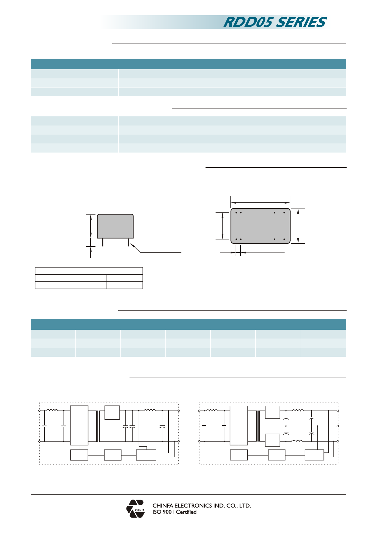
PHYSICAL CHARACTERISTICS
Case size
Case material
Weight
Potting material
31.8 x 20.3 x 12.7 mm (1.25 x 0.8 x 0.5 inches)
Plastic
15 g
Epoxy
MECHANISM & PIN CONFIGURATION
mm [inch]
31.80 [1.25]
12.70 [0.50]
6.00 [0.24]
DIA 0.50 [0.02]
GENERAL TOLERANCE
0.00[0.00] - 30.00[1.18]
±0.30[0.01]
30.00[1.18] - 120.00[4.72]
±0.50[0.02]
15.24 [0.60]
23
9 11
23 22
16 14
2.54 [0.10]
BOTTOM VIEW
20.30 [0.80]
PIN ASSIGNMENT
GENERAL
PIN NO.
2&3
9
11
14
16
22 & 23
SINGLE
Vi -
NO PIN
N. C.
Vo+
Vo -
Vi+
DUAL
Vi -
com
Vo -
Vo+
com
Vi+
CIRCUIT SCHEMATIC
‧Block diagram for RDD05 series with single output
Vi +
Rectifier
Switching
Device
Vi -
Control
Opto -
Isolation
Reference &
Error Amp.
‧Block diagram for RDD05 series with dual output
Vo + Vi +
Vo - Vi -
Switching
Device
Control
Rectifier
Rectifier
Opto -
Isolation
Reference &
Error Amp.
Vo +
com
Vo -
www.chinfa.com
2014.05.26
sales@chinfa.com
P3
Share Link: 