K4S643233F 데이터 시트보기 (PDF) - Samsung
부품명
상세내역
제조사
K4S643233F Datasheet PDF : 8 Pages
| |||
K4S643233F-S(D)E/N/I/P
CMOS SDRAM
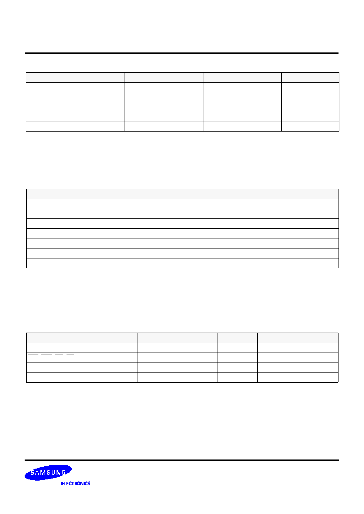
ABSOLUTE MAXIMUM RATINGS
Parameter
Symbol
Value
Voltage on any pin relative to Vss
VI N, VOUT
-1.0 ~ 4.6
Voltage on VD D supply relative to Vss
VDD , VDDQ
-1.0 ~ 4.6
Storage temperature
TSTG
-55 ~ +150
Power dissipation
PD
1
Short circuit current
IOS
50
Notes :
Permanent device damage may occur if ABSOLUTE MAXIMUM RATINGS are exceeded.
Functional operation should be restricted to recommended operating condition.
Exposure to higher than recommended voltage for extended periods of time could affect device reliability.
Unit
V
V
°C
W
mA
DC OPERATING CONDITIONS
Recommended operating conditions (Voltage referenced to VSS = 0V, TA = -25 °C to 85 °C for Extended, -40°C to 85°C for Industrial)
Parameter
Supply voltage
Input logic high voltage
Input logic low voltage
Output logic high voltage
Output logic low voltage
Input leakage current
Symbol
VD D
VDDQ
VI H
VIL
VO H
VOL
IL I
Min
2.7
2.7
2.2
-0.3
2.4
-
-10
Typ
Max
Unit
3.0
3.6
V
3.0
3.6
V
3.0
VDDQ+0.3
V
0
0.5
V
-
-
V
-
0.4
V
-
10
uA
Note
1
2
IOH = -2mA
IOL = 2mA
3
Notes :
1. VIH (max) = 5.3V AC. The overshoot voltage duration is ≤ 3ns.
2. VIL (min) = -2.0V AC. The undershoot voltage duration is ≤ 3ns.
3. Any input 0V ≤ VIN ≤ VDDQ.
Input leakage currents include HI-Z output leakage for all bi-directional buffers with Tri-State outputs.
4. Dout is disabled, 0V ≤ VOUT ≤ VDDQ.
CAPACITANCE (VDD = 3.0V & 3.3, TA = 23°C, f = 1MHz, VREF =0.9V ± 50 mV)
Pin
Symbol
Min
Clock
CCLK
-
RAS, CAS, WE, CS, CKE, DQM0~ DQM3
CIN
-
Address(A0 ~ A10, BA0 ~ BA1)
CADD
-
D Q0 ~ D Q31
COUT
-
Max
4.0
4.0
4.0
6.0
Unit
pF
pF
pF
pF
Note
Rev. 1.5 Dec. 2002
Share Link: 