K6R1016V1C 데이터 시트보기 (PDF) - Samsung
부품명
상세내역
제조사
K6R1016V1C Datasheet PDF : 11 Pages
| |||
K6R1016V1C-C/C-L, K6R1016V1C-I/C-P
for AT&T
CMOS SRAM
*DC AND OPERATING CHARACTERISTICS*(TA=0 to 70°C, Vcc=3.3V+0.3V/-0.15V, unless otherwise specfied)
Parameter
Symbol
Test Conditions
Min
Max
Unit
Input Leakage Current
ILI
VIN=VSS to VCC
-2
2
µA
Output Leakage Current
ILO
CS=VIH or OE=VIH or WE=VIL
VOUT=VSS to VCC
-2
2
µA
Operating Current
ICC
Min. Cycle, 100% Duty
10ns
-
CS=VIL, VIN = VIH or VIL, IOUT=0mA
12ns
-
105
mA
95
15ns
-
93
20ns
-
90
Standby Current
ISB
Min. Cycle, CS=VIH
-
30
mA
ISB1
f=0MHz, CS ≥VCC-0.2V,
VIN≥VCC-0.2V or VIN ≤0.2V
Normal
-
L-Ver.
-
5
mA
0.5
Output Low Voltage Level
VOL
IOL=8mA
-
0.4
V
Output High Voltage Level
VOH
IOH=-4mA
* The above parameters are also guaranteed at industrial temperature range.
2.4
-
V
CAPACITANCE*(TA=25°C, f=1.0MHz)
Item
Input/Output Capacitance
Input Capacitance
Symbol
CI/O
CIN
Test Conditions
MIN
VI/O=0V
-
VIN=0V
-
Max
8
6
Unit
pF
pF
* Capacitance is sampled and not 100% tested.
AC CHARACTERISTICS(TA=0 to 70°C, Vcc=3.3V+0.3V/-0.15V, unless otherwise noted.)
TEST CONDITIONS*
Parameter
Input Pulse Levels
Input Rise and Fall Times
Input and Output timing Reference Levels
Output Loads
Value
0V to 3V
3ns
1.5V
See below
* The above test conditions are also applied at industrial temperature range.
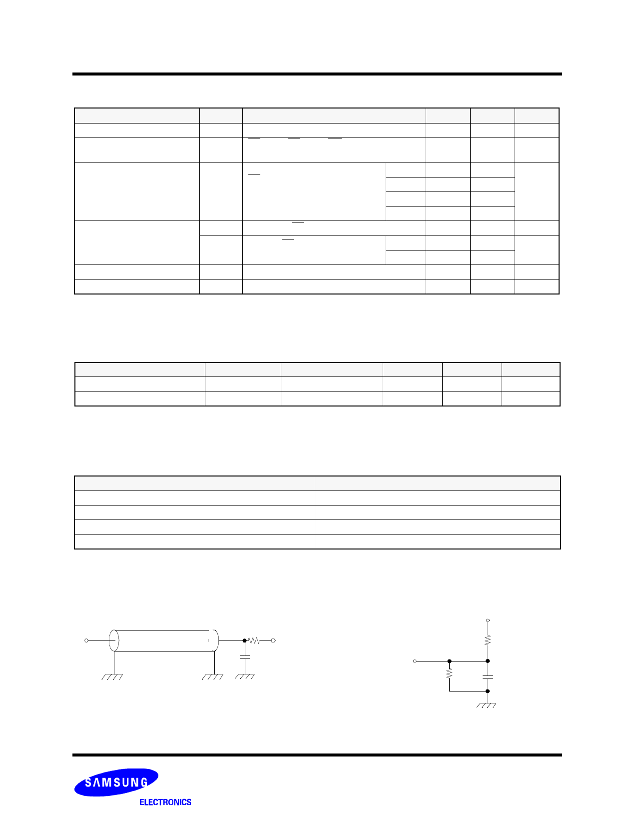
Output Loads(A)
DOUT
ZO = 50Ω
RL = 50Ω
VL = 1.5V
30pF*
Output Loads(B)
for tHZ, tLZ, tWHZ, tOW, tOLZ & tOHZ
DOUT
353Ω
+3.3V
319Ω
5pF*
* Capacitive Load consists of all components of the
test environment.
-4-
* Including Scope and Jig Capacitance
Revision 3.3
October 2000
Share Link: 