L6243 데이터 시트보기 (PDF) - STMicroelectronics
부품명
상세내역
제조사
L6243 Datasheet PDF : 12 Pages
| |||
L6243-L6243D
BLOCK DESCRIPTION
OUTPUT STAGE
It consists of two Power Op Amps connected in
bridge configuration.
CURRENT SENSE AMPLIFIER
Differential amplifier whose inputs are connected
to the sense lines and whose output is accessible
externally. Closing the loop will transform the
differential voltage signal from the sense lines into
a current signal for the Error Amplifier.
ERROR AMPLIFIER
Error amplifier which drives the output stage. The
input and the output pins are accessible exter-
nally.
POWER SUPPLY MONITOR OPERATION
The circuit monitors the logic supply voltage input
(typ 5V) and activates Power on Reset and Write
Disable output when such a supply drops below
the safe operating limit. After the logic supply volt-
age reaches its nominal value a delay capacitor
has to be charged [Tdelay=3x10e5 x C sec] be-
fore Power on Reset and Write Disable outputs
change from low to high level. Falling edges of
Write Disable and Power on Reset are delayed
(typ 4µs) in order to disable the writing on the disk
before the Power on Reset is activated. An addi-
tional supervisor circuit is present in the IC with a
programmable threshold, which is set by an exter-
nal resistive divider. The TTL compatible output
can be used separately or connected to Park in-
put in order to park the head.
The VCC sense output pin can also be connected
to 5V filter input in order to implement a POWER
ON RESET function sensitive both to 5V and VCC.
PARKING CIRCUIT OPERATIONT
The voice coil driver is switched into the parking
condition when Power on Reset output or Park in-
put are low. In such a condition a fixed voltage is
superimposed on the load and the value of such a
voltage is set by connecting an external resistor
between Park Voltage Program input and
ground: (Vpark=Rext x Iref, Iref=100µA typ). Con-
necting ENABLE input to GND the driver will be
disabled (outputs in high impedance mode).
THERMAL SHUTDOWN
It will disable the IC when the junction tempera-
ture exceeds the threshold value above which the
device could be damaged.
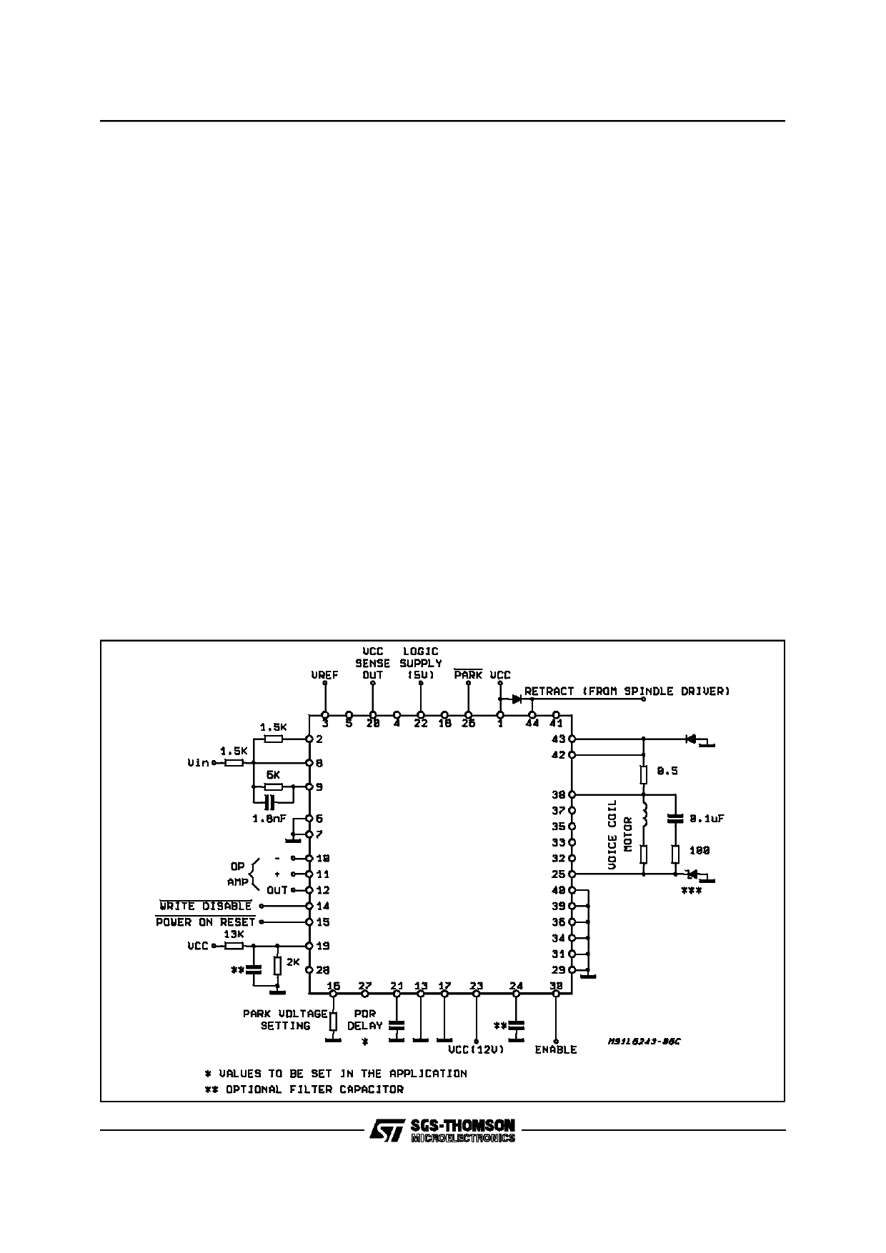
Figure 1: Application Circuit (The pinout refers to the L6243)
7/12
Share Link: 