L5987 데이터 시트보기 (PDF) - STMicroelectronics
부품명
상세내역
제조사
L5987 Datasheet PDF : 40 Pages
| |||
Pin settings
1
Pin settings
1.1
Pin connection
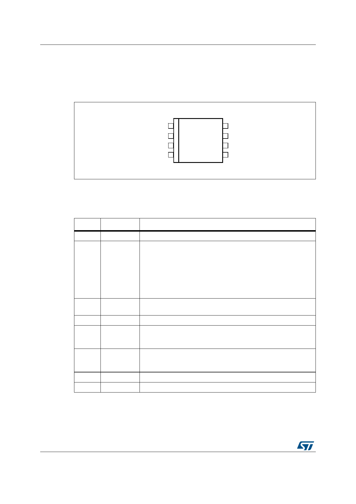
Figure 2. Pin connection (top view)
OUT
SYNCH
INH
COMP
VCC
GND
FSW
FB
L5987
1.2
Pin description
Table 1. Pin description
No.
Type
Description
1
OUT
Regulator output
Master/slave synchronization. When it is left floating, a signal with
a phase shift of half a period with respect to the power turn-on is present
at the pin. When connected to an external signal at a frequency higher
2
SYNCH
than the internal one, then the device is synchronized by the external
signal, with zero phase shift.
Connecting together the SYNCH pin of two devices, the one with higher
frequency works as a master and the other one as a slave; so the two
powers turn-on have a phase shift of half a period.
3
INH
A logical signal (active high) disables the device. With INH higher than
1.9 V the device is OFF and with INH lower than 0.6 V the device is ON.
4
COMP Error amplifier output to be used for loop frequency compensation
Feedback input. Connecting the output voltage directly to this pin the
5
FB
output voltage is regulated at 0.6 V. To have higher regulated voltages an
external resistor divider is required from the Vout to the FB pin.
The switching frequency can be increased connecting an external
6
FSW
resistor from the FSW pin and ground. If this pin is left floating, the device
works at its free-running frequency of 250 kHz.
7
GND
Ground
8
VCC
Unregulated DC input voltage
4/40
DocID14972 Rev 4
Share Link: 