L5987 데이터 시트보기 (PDF) - STMicroelectronics
부품명
상세내역
제조사
L5987 Datasheet PDF : 40 Pages
| |||
Functional description
5
Functional description
L5987
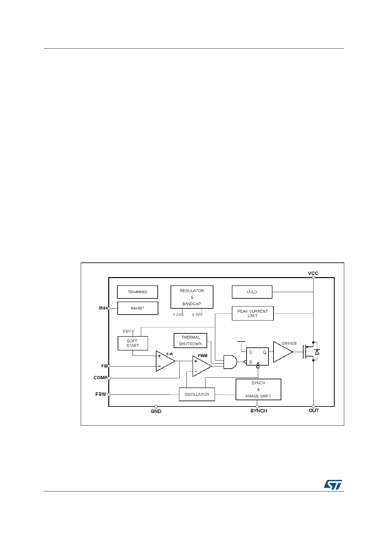
The L5987 device is based on a “voltage mode”, constant frequency control. The output
voltage VOUT is sensed by the feedback pin (FB) compared to an internal reference (0.6 V)
providing an error signal that, compared to a fixed frequency sawtooth, controls the ON and
OFF time of the power switch.
The main internal blocks are shown in the block diagram in Figure 3. They are:
A fully integrated oscillator that provides sawtooth to modulate the duty cycle and the
synchronization signal. Its switching frequency can be adjusted by an external resistor.
The voltage and frequency feedforward are implemented.
The soft-start circuitry to limit inrush current during the startup phase.
The voltage mode error amplifier.
The pulse width modulator and the relative logic circuitry necessary to drive the internal
power switch.
The high-side driver for an embedded P-channel Power MOSFET switch.
The peak current limit sensing block, to handle overload and short-circuit conditions.
A voltage regulator and internal reference. It supplies internal circuitry and provides
a fixed internal reference.
A voltage monitor circuitry (UVLO) that checks the input and internal voltages.
A thermal shutdown block, to prevent thermal runaway.
Figure 3. Block diagram
8/40
DocID14972 Rev 4
Share Link: 