LA7265W(1998) 데이터 시트보기 (PDF) - SANYO -> Panasonic
부품명
상세내역
제조사
LA7265W Datasheet PDF : 24 Pages
| |||
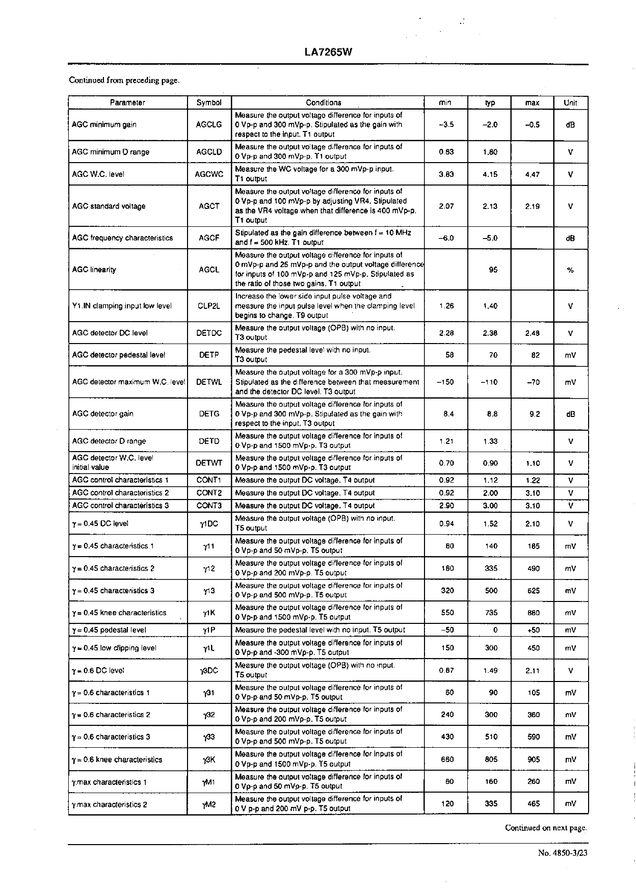
LA7265W
Continued from preceding page.
Parameter
AGC minimum gain
AGC minimum D range
AGC W.C. level
Symbol
AGCLG
AGCLD
AGCWC
AGC standard voltage
AGCT
AGC frequency characteristics
AGCF
AGC linearity
AGCL
Y1.IN clamping input low level
CLP2L
AGC detector DC level
AGC detector pedestal level
DETDC
DETP
AGC detector maximum W.C. level DETWL
AGC detector gain
AGC detector D range
AGC detector W.C. level
initial value
AGC control characteristics 1
AGC control characteristics 2
AGC control characteristics 3
γ = 0.45 DC level
γ = 0.45 characteristics 1
γ = 0.45 characteristics 2
γ = 0.45 characteristics 3
γ = 0.45 knee characteristics
γ = 0.45 pedestal level
γ = 0.45 low clipping level
γ = 0.6 DC level
γ = 0.6 characteristics 1
γ = 0.6 characteristics 2
γ = 0.6 characteristics 3
γ = 0.6 knee characteristics
γ.max characteristics 1
γ.max characteristics 2
DETG
DETD
DETWT
CONT1
CONT2
CONT3
γ1DC
γ11
γ12
γ13
γ1K
γ1P
γ1L
γ3DC
γ31
γ32
γ33
γ3K
γM1
γM2
Conditions
Measure the output voltage difference for inputs of
0 Vp-p and 300 mVp-p. Stipulated as the gain with
respect to the input. T1 output
Measure the output voltage difference for inputs of
0 Vp-p and 300 mVp-p. T1 output
Measure the WC voltage for a 300 mVp-p input.
T1 output
Measure the output voltage difference for inputs of
0 Vp-p and 100 mVp-p by adjusting VR4. Stipulated
as the VR4 voltage when that difference is 400 mVp-p.
T1 output
Stipulated as the gain difference between f = 10 MHz
and f = 500 kHz. T1 output
Measure the output voltage difference for inputs of
0 mVp-p and 25 mVp-p and the output voltage difference
for inputs of 100 mVp-p and 125 mVp-p. Stipulated as
the ratio of those two gains. T1 output
Increase the lower side input pulse voltage and
measure the input pulse level when the clamping level
begins to change. T9 output
Measure the output voltage (OPB) with no input.
T3 output
Measure the pedestal level with no input.
T3 output
Measure the output voltage for a 300 mVp-p input.
Stipulated as the difference between that measurement
and the detector DC level. T3 output
Measure the output voltage difference for inputs of
0 Vp-p and 300 mVp-p. Stipulated as the gain with
respect to the input. T3 output
Measure the output voltage difference for inputs of
0 Vp-p and 1500 mVp-p. T3 output
Measure the output voltage difference for inputs of
0 Vp-p and 1500 mVp-p. T3 output
Measure the output DC voltage. T4 output
Measure the output DC voltage. T4 output
Measure the output DC voltage. T4 output
Measure the output voltage (OPB) with no input.
T5 output
Measure the output voltage difference for inputs of
0 Vp-p and 50 mVp-p. T5 output
Measure the output voltage difference for inputs of
0 Vp-p and 200 mVp-p. T5 output
Measure the output voltage difference for inputs of
0 Vp-p and 500 mVp-p. T5 output
Measure the output voltage difference for inputs of
0 Vp-p and 1500 mVp-p. T5 output
Measure the pedestal level with no input. T5 output
Measure the output voltage difference for inputs of
0 Vp-p and -300 mVp-p. T5 output
Measure the output voltage (OPB) with no input.
T5 output
Measure the output voltage difference for inputs of
0 Vp-p and 50 mVp-p. T5 output
Measure the output voltage difference for inputs of
0 Vp-p and 200 mVp-p. T5 output
Measure the output voltage difference for inputs of
0 Vp-p and 500 mVp-p. T5 output
Measure the output voltage difference for inputs of
0 Vp-p and 1500 mVp-p. T5 output
Measure the output voltage difference for inputs of
0 Vp-p and 50 mVp-p. T5 output
Measure the output voltage difference for inputs of
0 V p-p and 200 mV p-p. T5 output
min
–3.5
0.63
3.83
2.07
–6.0
1.26
2.28
58
–150
8.4
1.21
0.70
0.92
0.92
2.90
0.94
80
180
320
550
–50
150
0.87
60
240
430
660
60
120
Ratings
Unit
typ
max
–2.0
–0.5
dB
1.80
V
4.15
4.47
V
2.13
2.19
V
–5.0
dB
95
%
1.40
2.38
70
–110
V
2.48
V
82
mV
–70
mV
8.8
9.2
dB
1.33
V
0.90
1.10
V
1.12
1.22
V
2.00
3.10
V
3.00
3.10
V
1.52
2.10
V
140
185
mV
335
490
mV
500
625
mV
735
880
mV
0
+50
mV
300
450
mV
1.49
2.11
V
90
105
mV
300
360
mV
510
590
mV
805
905
mV
160
260
mV
335
465
mV
Continued on next page.
No. 4850-3/24
Share Link: 