LB11993W 데이터 시트보기 (PDF) - SANYO -> Panasonic
부품명
상세내역
제조사
LB11993W Datasheet PDF : 15 Pages
| |||
LB11993W
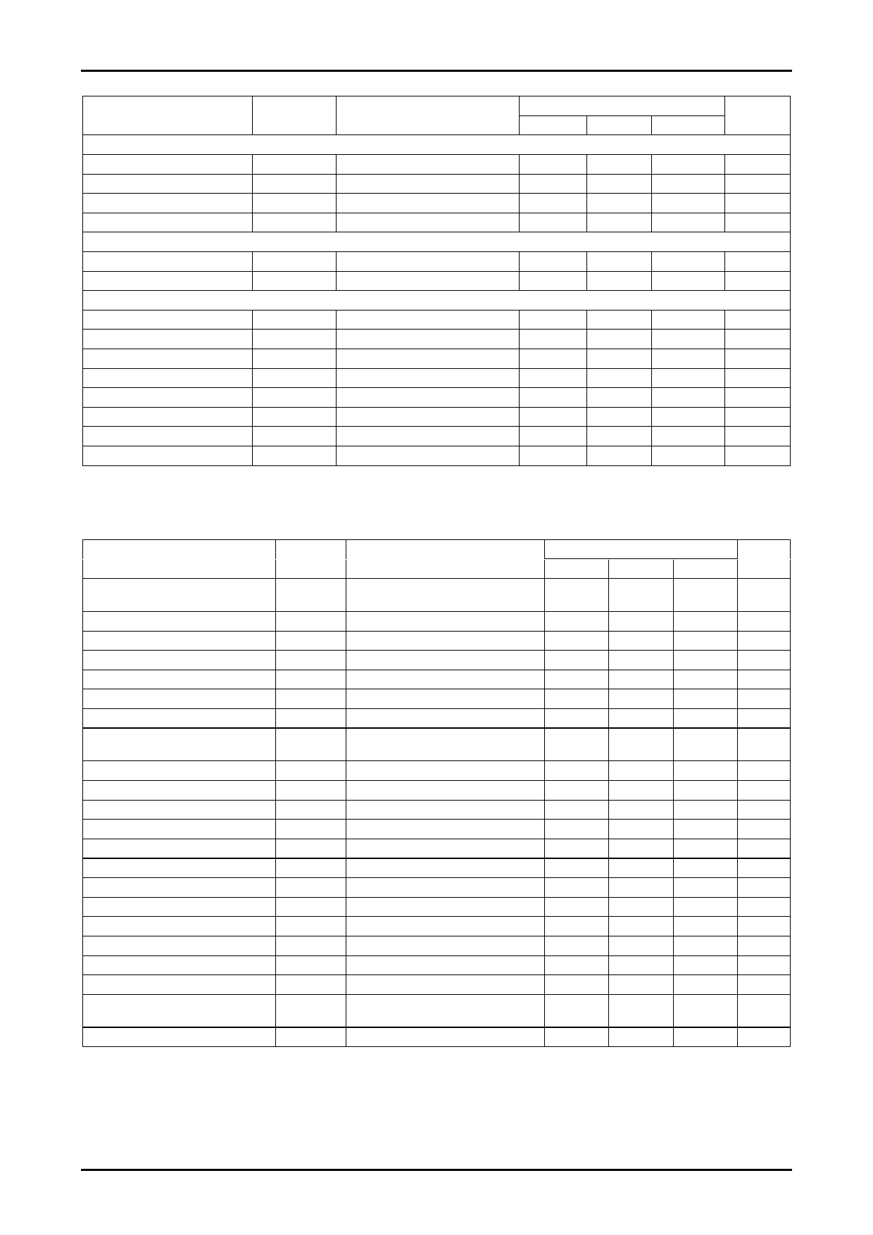
Continued from preceding page.
Parameter
Symbol
Conditions
Ratings
Unit
min
typ
max
[FRC pin]
High-level voltage
Low-level voltage
VFRCH
VFRCL
2.5
VCC1
V
-0.2
0.4
V
Input current
IFRCIN
VFRC_C=3V
20
40
µA
Leakage current
IFRCLK
VFRC_C=0V
-30
µA
[VH]
Hall supply voltage
Minus (-) pin voltage
[FG comparator]
VHALL
VH(-)
IH=5mA, VH(+)-VH(-)
IH=5mA
0.83
0.93
0.90
0.97
1.03
V
1.04
V
Input offset voltage
VFGOFF
-3
+3
mV
Input bias current
IbFG
VFGIN+=VFGIN-=1.5V
500
nA
Input bias current offset
∆IbFG
VFGIN+=VFGIN-=1.5V
-100
100
nA
Common-mode input range
VFGCM
1.2
2.5
V
High-level output voltage
VFGOH
When internally pulled up
2.8
V
Low-level output voltage
VFGOL
When internally pulled up
0.2
V
Voltage gain
VGFG
Design target value, Note 1
100
dB
Output current (sink)
IFGOs
Output pin set to low
5
mA
Note 1: Design target value parameters are not tested.
Note 2: The standard for the overlap amount parameter is to report the measured value without change.
Cylinder Motor Driver Block at Ta=25°C, VCC1=3V, VCC2=4.75V, VS=3V
Parameter
Symbol
Conditions
Supply current 4
Output quiescent current 4
Output quiescent current 5
ICC2
ICC2Q
IS(D)Q
IO=76mA, VSTBY_D=3V
VSTBY_C=0V
VSTBY_D=VSTBY_C=0V
VSTBY_D=VSTBY_C=0V
Output saturation voltage upper side 1
Output saturation voltage lower side 1
Output saturation voltage upper side 2
Output saturation voltage lower side 2
COM pin common-mode input voltage
range
Standby pin high-level voltage
VOU1
VOD1
VOU2
VOD2
VIC
VSTBYH
IO=0.1A, RF=0.25Ω
IO=0.1A, RF=0.25Ω
IO=0.4A, VS=3V, RF=0.25Ω
IO=0.4A, VS=3V, RF=0.25Ω
Standby pin low-level voltage
VSTBYL
Standby pin input current
ISTBYH
VSTBY_D=3V
Standby pin leakage current
ISTBYL
VSTBY_D=0V
FRC pin high-level voltage
VFRCH
FRC pin low-level voltage
VFRCL
FRC pin input current
IFRCI
VFRC_D=3V
FRC pin leakage current
IFRCL
VFRC_D=0V
Slope pin source current ratio
RSOURCE ICSLP1SOURCE/ICSLP2SOURCE
Slope pin sink current ratio
RSINK
ICSLP1SINK/ICSLP2SINK
CSLP1 source-to-sink current ratio
RCSLP1
ICSLP1SOURCE/ICSLP1SINK
CSLP2 source-to-sink current ratio
RCSLP2
ICSLP2SOURCE/ICSLP2SINK
Startup frequency
Phase delay width
Freq
Dwidth
Cosc=0.1µF, OSC frequency
Design target value, Note 1
Design target value, Note 1
Note 1: Design target value parameters are not tested.
Ratings
Unit
min
typ
max
0.75
2.5
mA
100
µA
100
300
µA
0.2
0.4
V
0.2
0.4
V
0.3
0.6
V
0.3
0.6
V
0.3
VCC2-0.9
V
2
VCC1
V
-0.2
0.7
V
50
µA
-10
µA
2
VCC1
V
-0.2
0.7
V
50
µA
-10
µA
-20
20
%
-20
20
%
-35
15
%
-35
15
%
11.5
Hz
30
deg
No.A0677-3/15
Share Link: 