LB11993W 데이터 시트보기 (PDF) - SANYO -> Panasonic
부품명
상세내역
제조사
LB11993W Datasheet PDF : 15 Pages
| |||
LB11993W
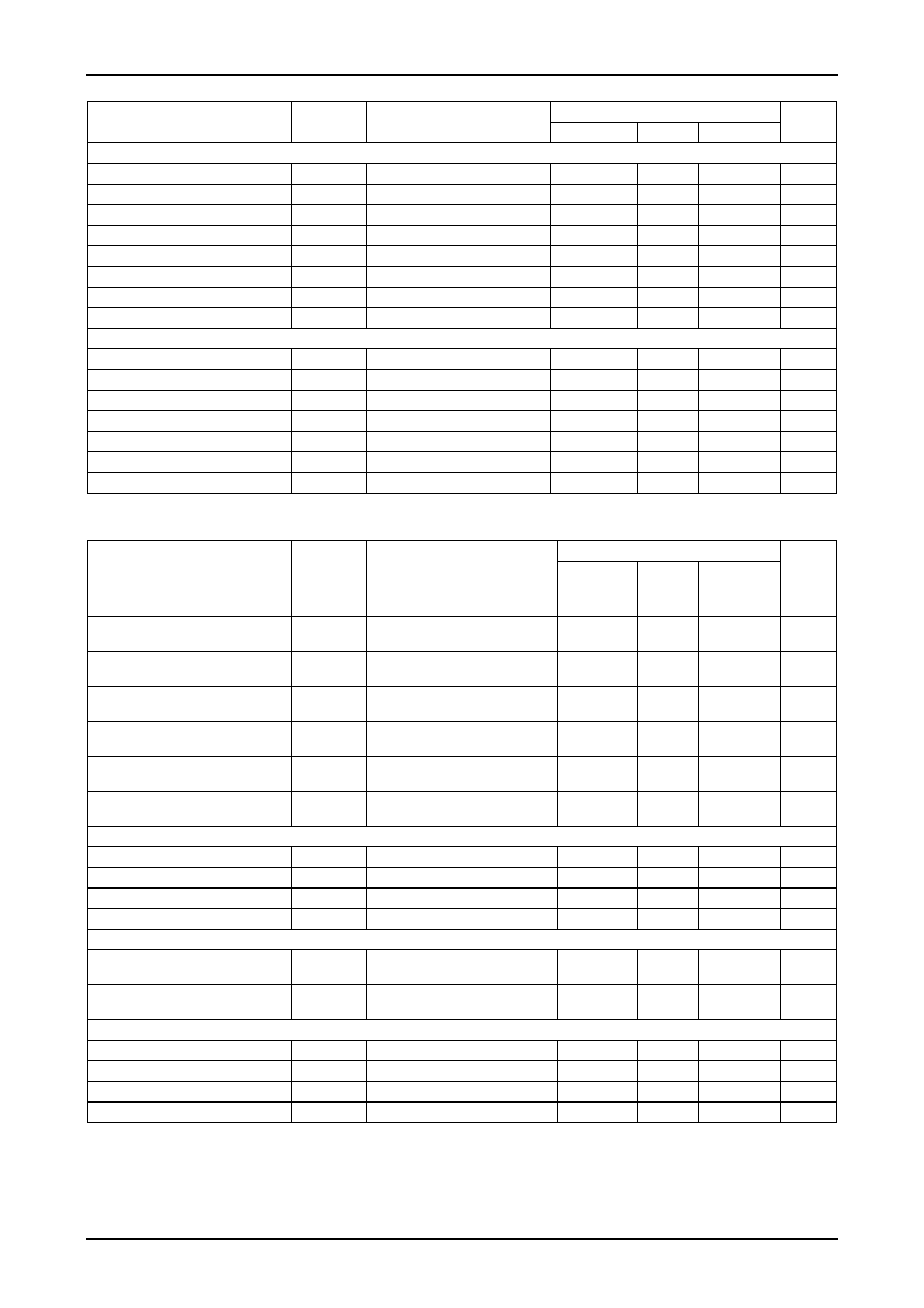
FG and PG Amplifier Blocks at Ta=25°C, VCC1=3V, VCC2=4.75V, VS=3V
Parameter
[FG amplifier]
Input offset voltage
Input bias current
Common-mode input voltage range
Open loop gain
Output ON voltage
Output OFF voltage
Schmitt amplifier hysteresis width
Reference voltage
[PG amplifier]
Input offset voltage
Input bias current
Common-mode input voltage range
Open loop gain
Output ON voltage
Output OFF voltage
Schmitt amplifier hysteresis width
Symbol
Conditions
VIO
IBIN-
VICOM
GVFG
VOL
VOH
VSHIS
VREF
VIO
IBIN-
VICOM
GVPG
VOL
VOH
VSHIS
f=1kHz
When IO=10µA
When IO=10µA
f=1kHz
When IO=10µA
When IO=10µA
min
1
VCC1-0.5
1.30
1
VCC1-0.5
Ratings
typ
±1
55
50
1.40
±1
55
50
Unit
max
±5
mV
250
nA
2
V
dB
0.4
V
V
mV
1.50
V
±5
mV
250
nA
2
V
dB
0.4
V
V
mV
Loading Motor Driver Block at Ta=25°C, VCC1=3V, VCC2=4.75V, VS=3V
Parameter
VCC1 supply current 1
VCC1 supply current 2
VCC1 supply current 3
VCC2 supply current 1
VCC2 supply current 2
VCC2 supply current 3
VS_L supply current
Symbol
ICC11
ICC12
ICC13
ICC21
ICC22
ICC23
IVS_L
[Logic inputs] (DEC1 and DEC2 pins)
High-level input voltage
High-level influx current
Low-level input voltage
Low-level influx current
[Loading motor driver]
Output saturation voltage 1
VINH
IINH
VINL
IINL
VOH
Output saturation voltage 2
VSHIS
[OP-AMP1, OP-AMP2]
Input offset voltage
Input bias current
Common-mode input voltage range
Open loop gain
VIO
IB
VICM
GV1
Conditions
Standby mode
VSTBY_C=VSTBY_D=0V
Forward/reverse mode
VSTBYC=VSTBY_D=0V
Brake mode
VSTBYC=VSTBY_D=0V
Standby mode(VCC1=OPEN)
VSTBY_C, D=0V
Standby mode(VCC1=3.0V)
VSTBY_C, D=0V
Forward/reverse mode
VSTBY_C, D=0V
Standby mode
VSTBY_C, D=0V
VCC1=2.7 to 4.0V
VIN=3.0V
VCC1=2.7 to 4.0V
VIN=0.6V
IO=200mA
(upper and lower composition)
IO=400mA
(upper and lower composition)
min
2.0
-0.2
1
50
Ratings
typ
3.3
14
12
23
45
5
0.2
0.4
±1
55
Unit
max
5
mA
21
mA
18
mA
100
µA
100
µA
35
mA
20
µA
VCC1
V
100
µA
0.6
V
10
µA
0.3
V
0.6
V
±5
mV
1
µA
2
V
dB
Continued on next page.
No.A0677-4/15
Share Link: 