LC7219M 데이터 시트보기 (PDF) - SANYO -> Panasonic
부품명
상세내역
제조사
LC7219M Datasheet PDF : 12 Pages
| |||
LC7219, 7219M
Specifications
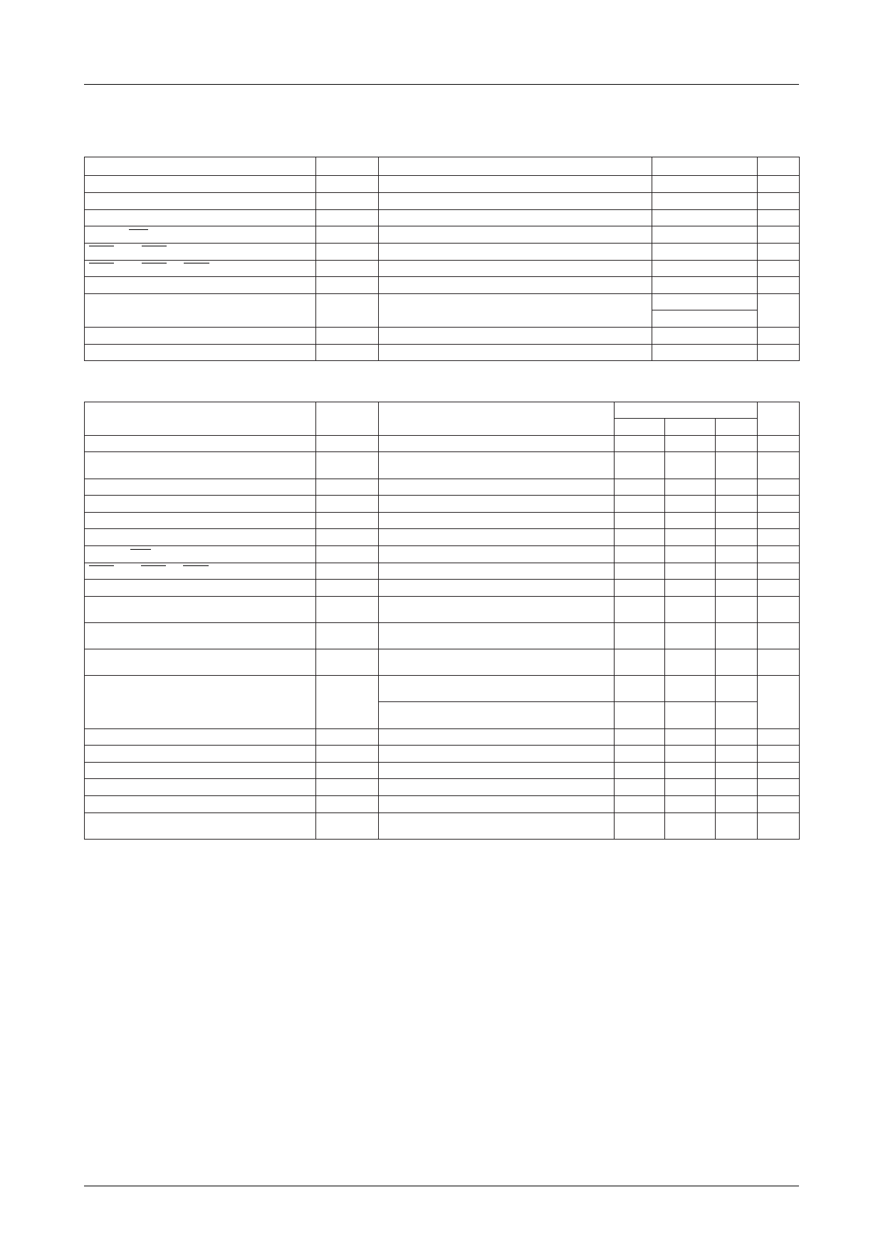
Absolute Maximum Ratings at Ta = 25˚C, VSS = 0V
Parameter
Symbol
Maximum supply voltage
CE, CL, DI, IN0 and IN1 input voltage
Input voltage for all other pins
DO and SYC output voltage
OUT1 and OUT2 output voltage
OUT0 and OUT3 to OUT6 output voltage
Output voltage for all other pins
VDD max
VIN1
VIN2
VOUT1
VOUT2
VOUT3
VOUT4
Allowable power dissipation
Pd max
Operating temperature
Storage temperature
Topr
Tstg
Conditions
Ratings
Unit
– 0.3 to +7.0 V
– 0.3 to +7.0 V
– 0.3 to VDD+0.3 V
– 0.3 to +7.0 V
– 0.3 to VDD+0.3 V
– 0.3 to +15.0 V
– 0.3 to VDD+0.3 V
350 (LC7219)
mW
350 (LC7219M)
– 40 to +85 ˚C
– 55 to +125 ˚C
Reommended Operating Conditions at Ta = 25˚C, VSS = 0V
Parameter
Symbol
Conditions
Supply voltage range
Supply voltage range for crystal oscillator
operation
CE, CL, DI, IN0 and IN1 high-level input voltage
LCTR high-level iutput voltage
CL, CE, DI, IN0 and IN1 low-level input voltage
LCTR low-level iutput voltage
DO and SYC output voltage
OUT0 and OUT3 to OUT6 output voltage
XIN input frequency
FMIN input frequency*1
AMIN input frequency
HCTR input frequency*2
VDD1
VDD2
VIH1
VIH2
VIL1
VIL2
VOUT1
VOUT2
fIN1
fIN2
fIN3
fIN4
LCTR input frequency
fIN5
Crystal oscillator frequency
XIN rms input amplitude
FMIN rms input amplitude*1
AMIN rms input amplitude
HCTR rms input amplitude*2
LCTR rms input amplitude
fXTAL
VIN1
VIN2
VIN3
VIN4
VIN5
Notes
1. fIN2=10 to 160MHz for VIN2=0.1V(min)
2. fIN4=10 to 70MHz for VIN4=0.1V(min)
VDD
VDD
Period measurement, VDD=4.5 to 6.5V
Period measurement, VDD=4.5 to 6.5V
Sine wave, capacitive coupling, VDD=3.5 to 6.5V
Sine wave, capacitive coupling, VDD=4.5 to 6.5V
See table 5
Sine wave, capacitive coupling, VDD=4.5 to 6.5V
See table 5
Priod measurement, sine wave, capacitive
coupling, VDD=4.5 to 6.5V
Frequency measurement, sine wave, capacitive
coupling, VDD=4.5 to 6.5V
Priod measurement, pulse wave DC coupling,
VDD=4.5 to 6.5V
XIN– XOUT: Crystal impedance ≤ 50Ω
Sine wave, capacitive coupling, VDD=4.5 to 6.5V
Sine wave, capacitive coupling, VDD=4.5 to 6.5V
Sine wave, capacitive coupling, VDD=4.5 to 6.5V
Frequency measurement, VDD=4.5 to 6.5V
Frequency measurement, sine wave, capacitive
coupling, VDD=4.5 to 6.5V
Ratings
min
typ
4.5
Unit
max
6.5 V
3.5
6.5 V
2.2
0.7VDD
0
0
1.0
6.5
VDD
0.7
0.3VDD
6.5
13
7.2
8.0
V
V
V
V
V
V
MHz
10
130 MHz
0.5
40.0 MHz
10
60 MHz
15
0.001
3.0
0.5
0.07
0.07
0.07
0.07
500
KHz
20.0
7.2
8.0 MHz
1.5 Vrms
1.5 Vrms
1.5 Vrms
1.5 Vrms
1.5 Vrms
No.3661–3/12
Share Link: 