LC7940KD 데이터 시트보기 (PDF) - SANYO -> Panasonic
부품명
상세내역
제조사
LC7940KD Datasheet PDF : 13 Pages
| |||
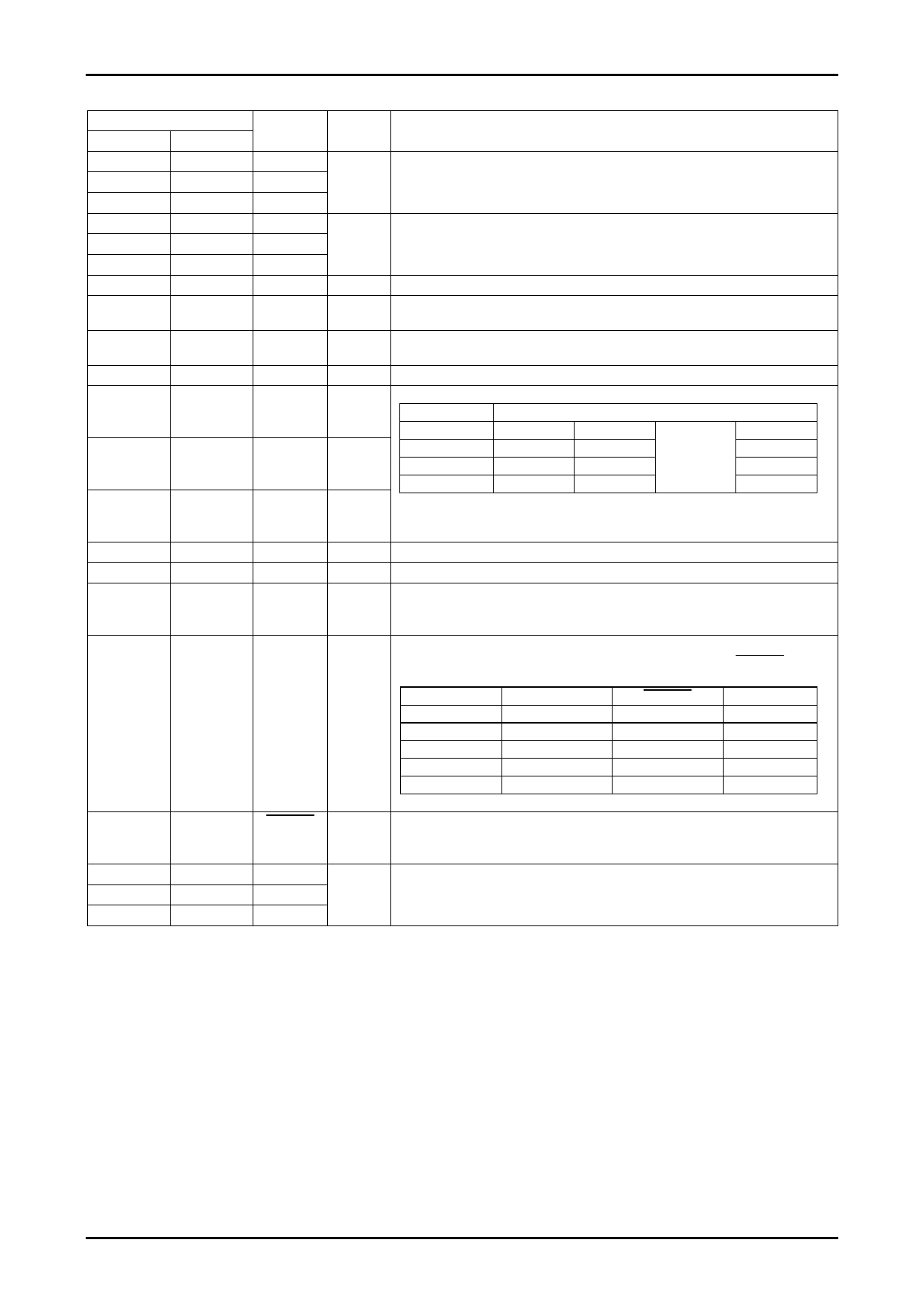
Pin Function
Pin No
LC7940KD
91
LC7941KDR
90
86
95
87
94
92
89
89
92
88
93
100
81
99
82
98
83
97
84
96
85
Symbol
VDD
VSS
VEE
V1
V3
V4
CP
CDI
LOAD
SDI
DI3
95
86
DI2
94
87
DI1
LC7940KD / LC7941KDR
I/O
Supply
Supply
I
I
I
I
I
I
I
Function
LCD panel drive voltage supplies
VDD-VSS is the logic supply.
VDD-VEE is the LCD supply.
LCD panel drive voltage supplies
V1 and VEE are selected levels.
V3 and V4 are not-selected levels.
Display data input clock (falling edge trigger).
Chip disable.
Data is read in When LOW, and not read in When HIGH.
Display data latch clock (falling edge trigger).
On the falling edge, the LCD drive signals set by the display data are output.
Serial data input.
4-bit parallel data input pins.
Data input
LCD driver output
SDI
O4
O8
O80
DI3
O3
O7
O79
→
DI2
O2
O6
O78
DI1
O1
O5
O77
In serial data input mode, DI1 to DI3 should all be tied HIGH or LOW.
93
85
82
1 to 80
84
81
83
90
88
M
96
P/S
99
CDO
80 to 1
O1 to O80
97
DISPOFF
91
NC
98
NC
100
NC
I
LCD panel drive voltage output alternation control signal.
I
Data input mode select. 4-bit parallel input when HIGH, and serial input when LOW.
O
Cascade connection pin for extension segment drivers.
Data is read out when HIGH. Goes LOW after data is read out.
Connected to the CDI input of the next chip.
O
LCD drive outputs.
The output drive level is determined by the display data, M signal and DISPOFF input
as shown below.
M
Q
DISPOFF
Output
L
L
H
V3
L
H
H
V1
H
L
H
V4
H
H
*
*
H
VEE
L
V1
Note* don’t care (tied HIGH or LOW)
I
O1 to O80 output control input pin.
When LOW, V1 is output on the O1 to O80 outputs.
See the truth table.
-
No connection.
No.A0573-5/13
Share Link: 