LC7940KD 데이터 시트보기 (PDF) - SANYO -> Panasonic
부품명
상세내역
제조사
LC7940KD Datasheet PDF : 13 Pages
| |||
LC7940KD / LC7941KDR
Electrical Characteristics at Ta = 25±2°C, VDD = 2.7 to 5.5V
Parameter
Symbol
Conditions
Ratings
Unit
min
typ
max
Input high level current
IIH
VIN = VDD: LOAD, CP, CDI, P/S, DI1 to DI3, SDI, M,
-
-
and DISPOFF
1
µA
Input low level current
IIL
VIN = VSS: LOAD, CP, CDI, P/S, DI1 to DI3, SDI, M,
and DISPOFF
-1
-
-
µA
Output high level voltage
Output low level voltage
VOH
VOL
IOH = -400µA: CDO
IOL = 400µA: CDO
VDD-0.4
-
-
-
-
V
0.4
V
Driver on resistance
RON
VDD-VEE = 18V, |VDE-Vo| = 0.25V *4
-
0.7
2
kΩ
Standby current drain
IST
CDI = VDD, VDD-VEE = 18V,
CP = 3.3MHz, Output unloaded: VSS
-
-
200
µA
Operating current drain
ISS *5 VDD-VEE = 18V, CP = 3.3MHz, LOAD = 5.156kHz
-
-
M = 52Hz: VSS
1.0
mA
IEE *6 VDD-VEE = 18V, CP = 3.3MHz, LOAD = 5.156kHz
-
-
M = 52Hz: VEE
0.1
mA
Note *4 VDE = one of V1, V3, V4 or VEE. V1 = VDD, V3 = 9/11(VDD-VEE), V4 = 2/11(VDD-VEE)
*5 ISS is the current flowing from VDD-VSS.
*6 IEE is the current flowing from VDD-VEE
Switching Characteristics at Ta = 25±2°C, VSS = 0V, VDD = 2.7 to 5.5V
Parameter
Output delay time
Symbol
tD
CL=30pF: CDO
Conditions
Ratings
Unit
min
typ
max
-
-
200
ns
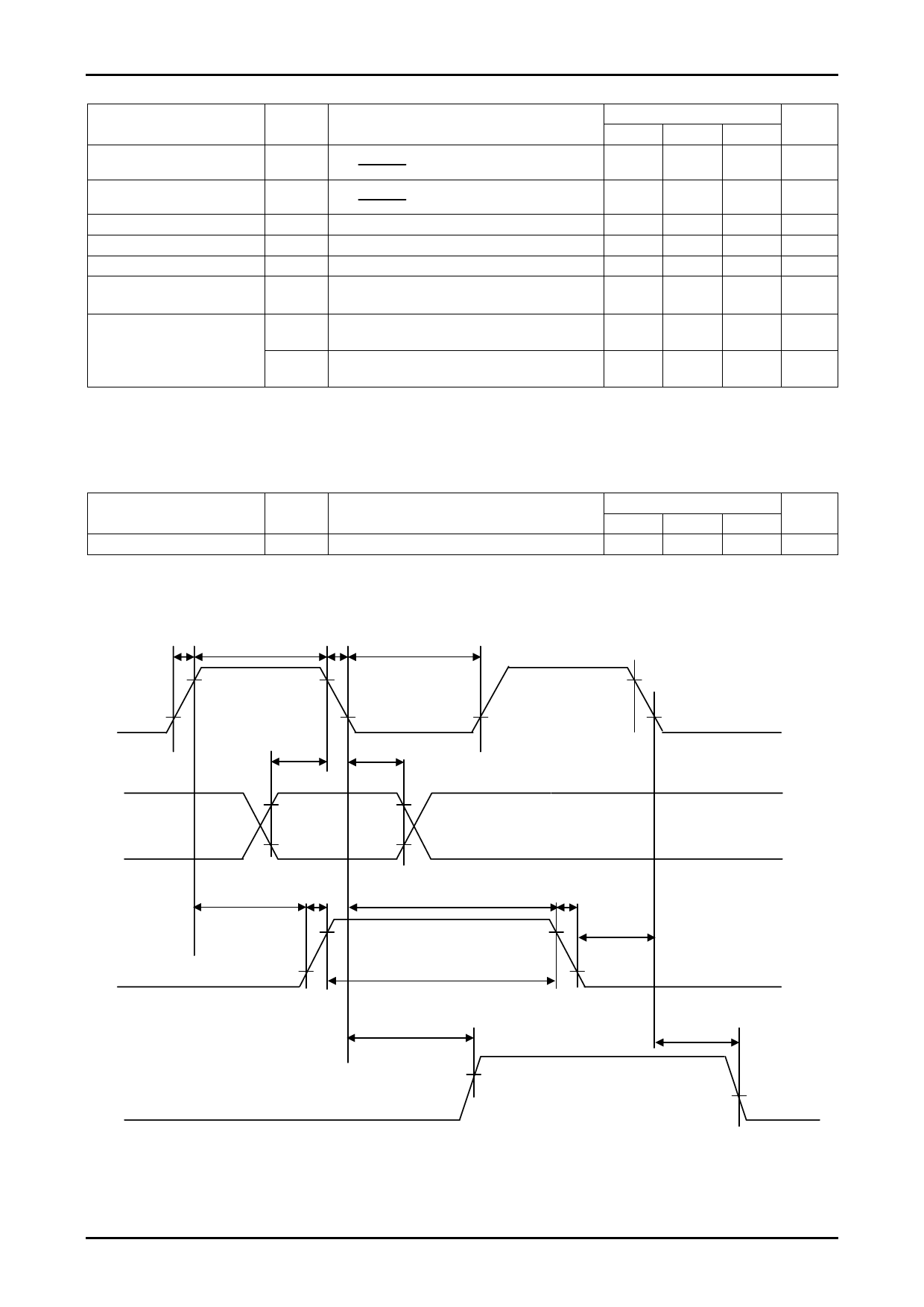
Switching Characteristics Diagram
tR
tWC
tF
tWC
0.8VDD
CP
0.2VDD
tSETUP
tHOLD
0.8VDD
0.2VDD
SDI
DI1 to 3
LOAD
0.8VDD
0.2VDD
tCL(1)
tRL
tCL(2)
tWL
tFL
tLC
CDO
tD
0.8VDD
tD
0.2VDD
No.A0573-7/13
Share Link: 