LM139 데이터 시트보기 (PDF) - STMicroelectronics
부품명
상세내역
제조사
LM139 Datasheet PDF : 10 Pages
| |||
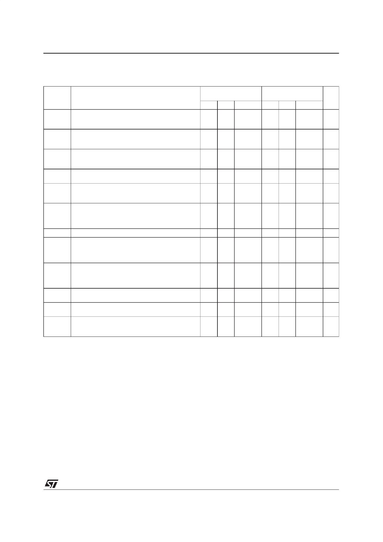
LM139,A - LM239,A - LM339,A
ELECTRICAL CHARACTERISTICS
VCC+ = +5V, VCC- = GND, Tamb = 25oC (unless otherwise specified)
Symbol
Parameter
Vio
Input Offset Voltage – (note 2)
Tamb = +25oC
Tmin. ≤ Tamb ≤ Tmax.
Iio
Input Offset Current
Tamb = +25oC
Tmin. ≤ Tamb ≤ Tmax.
Iib
Input Bias Current
Tamb = +25oC
(II+
or
II–)
-
(note
3)
Tmin. ≤ Tamb ≤ Tmax.
Avd Large Signal Voltage Gain
(VCC = 15V, RL =15kΩ, VO = 1 to 11V)
ICC Supply Current (all comparators)
VCC = +5V, no load
VCC = +30V, no load
Vicm Input Common Mode Voltage Range - (note 4)
(VCC
Tamb
=
=
30V)
+25oC
Tmin. ≤ Tamb ≤ Tmax.
Vid Differential Input Voltage - (note 6)
VOL Low Level Output Voltage
T(Vaimdb==-1+V2,5oIsCink = 4mA)
Tmin. ≤ Tamb ≤ Tmax.
IOH High Level Output Current ( Vid = 1V)
(VCC
Tamb
=
=
V+2O5=oC30V)
Tmin. ≤ Tamb ≤ Tmax.
Isink Output Sink Current
(Vid = -1V, VO = 1.5V)
tre
Response Time – (note 5)
(RL = 5.1kΩ connected to VCC+)
trel
Large Signal Response Time
(RL = 5.1kΩ connected to VCC+, eI = TTL,
V(ref) = +1.4V)
LM139A - LM239A
LM339A
LM139 - LM239
LM339
Unit
Min. Typ. Max. Min. Typ. Max.
1
2
4
mV
1
5
9
3
25
100
nA
5
50
150
25
100
300
50 200
1.1
2
1.3
2.5
25
50 200
1.1
1.3
nA
250
400
V/mV
mA
2
2.5
V
0
0
VVCCCC++-1-2.5
0
0
VVCCCC++-1-2.5
VCC+
VCC+
V
mV
250 400
700
250 400
700
0.1
1
6 16
1.3
300
0.1
6 16
1.3
nA
1
µA
mA
µs
ns
300
Notes :
2. A t out put sw it ch poi nt, VO ≈ 1. 4V , RS = 0 wi th VC C+ from 5V t o 30V, and over the full i nput common- mode r ange
(0V
to
V
C
+
C
–1.5V).
3. The di rect ion of the i nput curr ent i s out of t he IC due t o t he P N P i nput stage. This cur r ent is essent i al ly con-
stant, independent of the state of the output, so no loading charge exi sts on the reference of input lines.
4. The i nput common-mode vol t age of ei ther input si gnal volt age should not be al low ed t o go negati ve by more
than
0.3V.
T he
upper
end
of
the
co m mo n- m od e
v o l t ag e
r an ge
is
VC
+
C
– 1. 5 V,
but
e i th er
or
both
i np ut s
can
go
to +30V without damage.
5. The r esponse t ime speci fi ed i s f or a 100mV input st ep w i th 5mV overdri ve. For lar ger over dri ve signal s 300ns
can be obtained.
6. P osi t i ve excur si ons of i nput vol tage may exceed the power suppl y level . As long as the ot her vol t age r emai ns
within the common-mode range, the comparator will provide a proper output state. The low input voltage state
must not be less than –0.3V (or 0.3V bellow the negative power supply, i f used).
3/10
Share Link: 