LMV358(2005) 데이터 시트보기 (PDF) - Unisonic Technologies
부품명
상세내역
제조사
LMV358
(Rev.:2005)
(Rev.:2005)
Unisonic Technologies

LMV358 Datasheet PDF : 12 Pages
| |||
LMV358
LINEAR INTEGRATED CIRCUIT
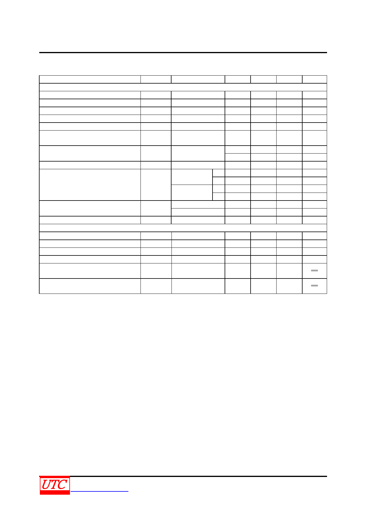
5V DC ELECTRICAL CHARACTERISTICS
Unless otherwise specified, all limits guaranteed for TJ =25°C, V1=5V, V=0V, VCM=2.0V, VOUT=V1/2 and RL>1MΩ.
Boldface limits apply at the temperature extremes.
PARAMETER
SYMBOL
CONDITIONS
MIN
TYP
MAX UNIT
Input Offset Voltage
Input Offset Voltage Average Drift
VOS
TCVos
7
1.7
9
mV
5
µV/°C
Input Bias Current
II(BIAS)
250
15
500
nA
Input Offset Current
Common Mode Rejection Ratio
Power Supply Rejection Ratio
II(OFF)
CMRR
PSRR
0V≦VCM≦4V
2.7V≦V1≦5V
VOUT=1V VCM=1V
50
5
150
nA
50
65
dB
50
60
dB
Input Common-Mode Voltage Range
VCM For CMRR≧50dB
0
-0.2
4.2
4
V
V
Large Signal Voltage Gain(Note 6)
Output Swing
Av
VOUT
RL=2kΩ
RL=2kΩ to 2.5V
RL=10kΩ to 2.5V
10
V+-400
300
V+-200
180
100
V1-40
120
V1-10
65
15
V1-300
400
V1-100
280
V/mV
mV
mV
mV
mV
Output Short Circuit Current
Supply Current
IOUT
Sourcing, VOUT =0V
Sinking, VOUT =5V
5
10
60
160
mA
mA
ISS Both amplifiers
440
210
615
µA
2.5V AC ELECTRICAL CHARACTERISTICS
Unless otherwise specified, all limits guaranteed for TJ =25°C, V1=2.7V, V=0V, VCM=2.0V, VOUT=V1/2 and RL>1MΩ
PARAMETER
SYMBOL
CONDITIONS
MIN
TYP
MAX UNIT
Slew Rate
SR
1
V/µs
Gain-Bandwidth Product
Phase Margin
GBWP CL=200pF
Φ(T)
1
MHz
60
Deg
Gain Margin
G(r)
10
dB
Input-Referred Voltage Noise
θr1 f=1kHz
nV
39
√ Hz
Input-referred Current Noise
Ir1 f=1kHz
0.21
pA
√ Hz
Note1: Absolute Maximum Ratings indicate limits beyond which damage to the device may occur. Operating Ratings
indicate conditions for which the device is intended to be functional, but specific performances is not
guaranteed. For guaranteed specifications and the test conditions, see the Electrical Characteristics.
Note2: Human body model 1.5kΩ in series with 100pF. Machine model, 0Ω in series with 200pF.
Note3: Shorting output to V1 will adversely after reliability.
Note4: Shorting output to V+ will adversely affect reliability.
Note5: The maximum power dissipation is a function of TJ(max) θJA and TA. The maximum allowable power
dissipation at any ambient temperature is PD=(TJ(max)-TA)/θJA. All numbers apply for packages soldered
directly into a PC board.
Note6: RL is connected to V. The output voltage is 0.5V≦VOUT≦4.5V.
Note7: Connected as voltage follower with 3V step input. Number specified is these lower of the positive and
negative slew rates.
Note8: all numbers are typical, and apply for packages soldered directly note a PC board is still air.
UNISONIC TECHNOLOGIES CO., LTD
www.unisonic.com.tw
4 of 12
QW-R105-010,C
Share Link: