LRS1386 데이터 시트보기 (PDF) - Sharp Electronics
부품명
상세내역
제조사
LRS1386 Datasheet PDF : 114 Pages
| |||
LRS1386
8
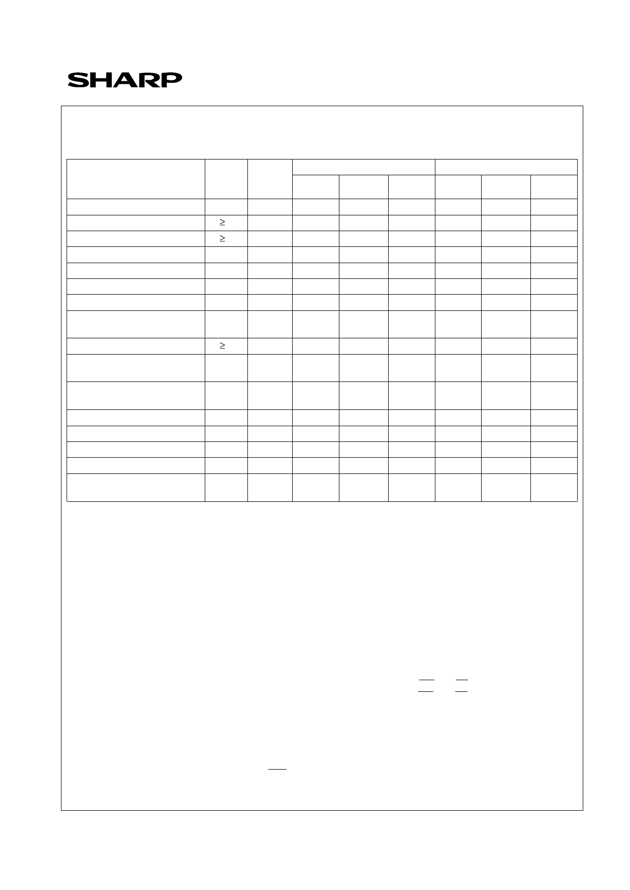
5. Command Definitions for Flash Memory(11)
5.1 Command Definitions
Command
Bus
Cycles
Req’d
Notes
First Bus Cycle
Oper(1) Address(2) Data(3)
Second Bus Cycle
Oper(1) Address(2) Data(3)
Read Array
1
2
Write
PA
FFH
Read Identifier Codes/OTP
2
2,3,4 Write
PA
90H
Read IA or OA ID or OD
Read Query
2
2,3,4 Write
PA
98H
Read
QA
QD
Read Status Register
2
2,3
Write
PA
70H
Read
PA
SRD
Clear Status Register
1
2
Write
PA
50H
Block Erase
2
2,3,5 Write
BA
20H
Write
BA
D0H
Full Chip Erase
2
2,5,9 Write
X
30H
Write
X
D0H
Program
2
2,3,5,6 Write
WA
40H or
10H
Write
WA
WD
Page Buffer Program
4 2,3,5,7 Write
WA
E8H
Write
WA
N-1
Block Erase and (Page Buffer)
Program Suspend
1
2,8,9 Write
PA
B0H
Block Erase and (Page Buffer)
Program Resume
1
2,8,9 Write
PA
D0H
Set Block Lock Bit
2
2
Write
BA
60H
Write
BA
01H
Clear Block Lock Bit
2
2,10 Write
BA
60H
Write
BA
D0H
Set Block Lock-down Bit
2
2
Write
BA
60H
Write
BA
2FH
OTP Program
2
2,3,9 Write
OA
C0H
Write
OA
OD
Set Partition Configuration
Register
2
2,3
Write PCRC
60H
Write PCRC
04H
Notes:
1. Bus operations are defined in 3.1 Bus operation.
2. First bus cycle command address should be the same as the second cycle address.
X=Any valid address within the device.
PA=Address within the selected partition.
IA=Identifier codes address (See 5.2, 5.3).
QA=Query codes address. Refer to the LH28F320BX, LH28F640BX series Appendix for details.
BA=Address within the block being erased, set/cleared block lock bit or set block lock-down bit.
WA=Address of memory location for the Program command or the first address for the Page Buffer Program command.
OA=Address of OTP block to be read or programmed (See 5.4 OTP Block Address Map).
PCRC=Partition configuration register code presented on the address A0-A15.
3. ID=Data read from identifier codes. (See 5.2, 5.3 ).
QD=Data read from query database. Refer to the LH28F320BX, LH28F640BX series Appendix for details.
SRD=Data read from status register. See 6. Status Register Definition for a description of the status register bits.
WD=Data to be programmed at location WA. Data is latched on the rising edge of F-WE or F-CE (whichever goes high first).
OD=Data to be programmed at location OA. Data is latched on the rising edge of F-WE or F-CE (whichever goes high first).
N-1=N is the number of the words to be loaded into a page buffer.
4. Following the Read Identifier Codes/OTP command, read operations access manufacturer code, device code, block lock
configuration code, partition configuration register code and the data within OTP block (See 5.2, 5.3 ).
The Read Query command is available for reading CFI (Common Flash Interface) information.
5. Block erase, full chip erase or (page buffer) program cannot be executed when the selected block is locked. Unlocked
block can be erased or programmed when F-RST is VIH.
6. Either 40H or 10H are recognized by the CUI (Command User Interface) as the program setup.
Share Link: 