LT1021 데이터 시트보기 (PDF) - Linear Technology
부품명
상세내역
제조사
LT1021 Datasheet PDF : 16 Pages
| |||
LT1021
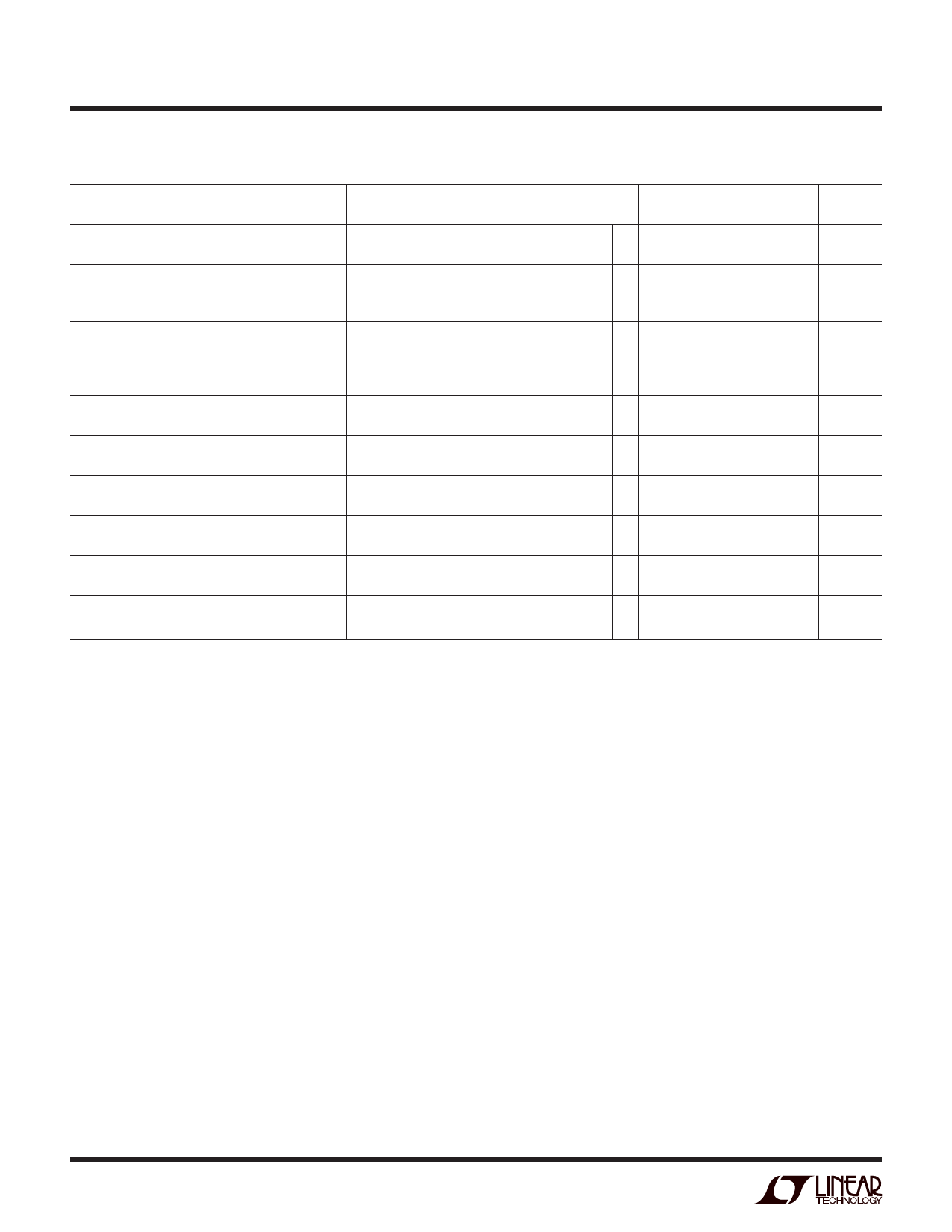
ELECTRICAL CHARACTERISTICS The q denotes specifications that apply over the full operating temperature
range, otherwise specifications are TA = 25°C. VIN = 15V, IOUT = 0, unless otherwise noted.
PARAMETER
Output Voltage (Note 2)
Output Voltage Temperature Coefficient (Note 3)
Line Regulation (Note 4)
Load Regulation (Sourcing Current)
Load Regulation (Shunt Mode)
Supply Current (Series Mode)
CONDITIONS
LT1021C-10
LT1021B-10/LT1021D-10
TMIN ≤ TJ ≤ TMAX
LT1021B-10
LT1021C-10/LT1021D-10
11.5V ≤ VIN ≤ 14.5V
14.5V ≤ VIN ≤ 40V
0 ≤ IOUT ≤ 10mA
(Note 4)
1.7mA ≤ ISHUNT ≤ 10mA
(Notes 4, 5)
Minimum Current (Shunt Mode)
Output Voltage Noise (Note 6)
Long Term Stability of Output Voltage (Note 7)
Temperature Hysteresis of Output
VIN is Open
0.1Hz ≤ f ≤ 10Hz
10Hz ≤ f ≤ 1kHz
∆t = 1000Hrs Noncumulative
∆T = ±25°C
LT1021-10
MIN TYP MAX
9.995 10.00 10.005
9.950 10.00 10.050
q
2
5
q
5
20
1.0
4
q
6
0.5
2
q
4
12
25
q
40
50
100
q
150
1.2
1.7
q
2.0
1.1
1.5
q
1.7
6.0
3.5
6
15
5
UNITS
V
V
ppm/°C
ppm/°C
ppm/V
ppm/V
ppm/V
ppm/V
ppm/mA
ppm/mA
ppm/mA
ppm/mA
mA
mA
mA
mA
µVP-P
µVRMS
ppm
ppm
Note 1: Absolute Maximum Ratings are those values beyond which the life
of a device may be impaired.
Note 2: Output voltage is measured immediately after turn-on. Changes
due to chip warm-up are typically less than 0.005%.
Note 3: Temperature coefficient is measured by dividing the change in
output voltage over the temperature range by the change in temperature.
Separate tests are done for hot and cold; TMIN to 25°C and 25°C to TMAX.
Incremental slope is also measured at 25°C.
Note 4: Line and load regulation are measured on a pulse basis. Output
changes due to die temperature change must be taken into account
separately. Package thermal resistance is 150°C/W for TO-5 (H), 130°C/W
for N and 150°C/W for the SO-8.
Note 5: Shunt mode regulation is measured with the input open. With the
input connected, shunt mode current can be reduced to 0mA. Load
regulation will remain the same.
Note 6: RMS noise is measured with a 2-pole highpass filter at 10Hz and a
2-pole lowpass filter at 1kHz. The resulting output is full-wave rectified and
then integrated for a fixed period, making the final reading an average as
opposed to RMS. Correction factors are used to convert from average to
RMS and correct for the non-ideal bandpass of the filters.
Peak-to-peak noise is measured with a single highpass filter at 0.1Hz and a
2-pole lowpass filter at 10Hz. The unit is enclosed in a still-air environment
to eliminate thermocouple effects on the leads. Test time is 10 seconds.
Note 7: Consult factory for units with long term stability data.
4
Share Link: 