EL4102C 데이터 시트보기 (PDF) - Elantec -> Intersil
부품명
상세내역
제조사
EL4102C Datasheet PDF : 9 Pages
| |||
EL4102C - Preliminary
500MHz Video Front End: 4-1 MUX, VGA & DC-Restore
Absolute Maximum Ratings (TA = 25°C)
Values beyond absolute maximum ratings can cause the device to be pre-
maturely damaged. Absolute maximum ratings are stress ratings only
and functional device operation is not implied.
Supply Voltage (VS+ to VS-)
11V
Input Voltage
VS- - 0.3V, VS+ +0.3V
Storage Temperature Range
Ambient operating Temperature
Operating Junction Temperature
Power Dissipation
-65°C to +150°C
-40°C to +85°C
125°C
See Curves
Important Note:
All parameters having Min/Max specifications are guaranteed. Typ values are for information purposes only. Unless otherwise noted, all tests are at the
specified temperature and are pulsed tests, therefore: TJ = TC = TA.
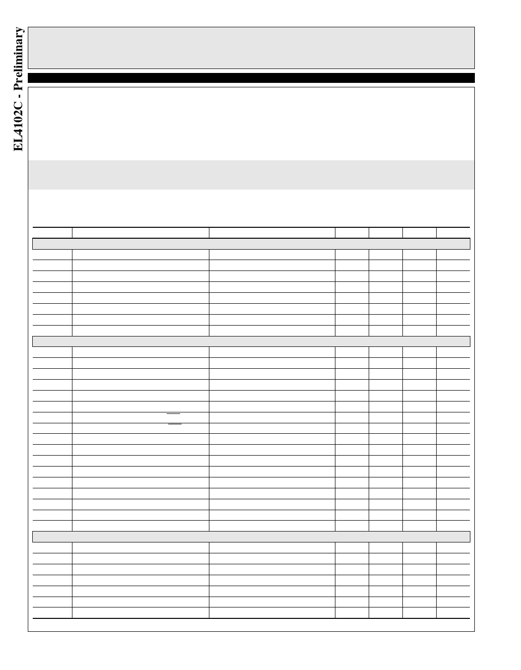
Electrical Characteristics
VS1+ = VS2+ = 5V, VS1- = VS2- = -5V, RFV = RFG = 750, RGV = RGM = O.C., AV = 1, RLV = RLM = 150Ω, CLV = CLM = 3p, CH = 0.33n, GAIN = 1.
Parameter
Supply
IS1+
IS-
IS2+
IS1S+
ISS-
IS2S+
VS1+, VS2+
VS-
Input
Ib
Ibo
VIH
VIL
VIP
VIN
IIDL
IIDH
IIL
IIH
tsh
tsu
th
Description
Positive Supply Current 1
Negative Supply Current
Positive Supply Current 2
Positive Supply Current 1 in Standby
Negative Supply Current in Standby
Positive Supply Current 2 in Standby
Positive Supply Voltage
Negative Supply Voltage
Input Bias Current
Input Bias Current Drift with Temp.
Input High Voltage
Input Low Voltage
Input Voltage Swing, Pos.
Input Voltage Swing, Neg.
Low Input Current for SCLK and ENB
High Input Current for SCLK and ENB
Low Input Current for SDI, PDWN, HOLD
High Input Current for SDI, PDWN, HOLD
Sample and Hold Delay Time
Data Set Up Time
Data Hold Time
Conditions
VIN = 0, IL = 0
VIN = 0, IL = 0
Standby
Standby
Standby
VIN = 0V
VIN = 0V
Saturated Input, Att. code = 01010
Saturated Input, Att. code = 01010
VIN = 0V
VIN =5V
VIN = 0V
VIN =5V
Min
14
3.8
0.57
-10
4.5
-4.5
-22.4
2
3.35
50
0
15
0
TBD
TBD
Typ
35
45
15
5
1
-
5.0
-5.0
-2.2
TBD
3.5
-3.5
85
0.1
48
0.1
15
10
10
Max
20
7.3
1.3
10
5.5
-5.5
6.1
0.8
-3.39
150
10
75
10
TBD
TBD
Unit
mA
mA
mA
mA
mA
µA
V
V
µA
nA/°C
V
V
V
V
µA
µA
µA
µA
ns
ns
ns
fclk
tsue
the
tpd
Output
VOSM
VOS
TCVOS
VO+
VO-
VSDO high
VSDO low
Serial Clock Rate
Enable Set Up Time
Enable Hold Time
Clock to Data Output Delay
Output Offset Voltage - Monitor
DC-restore Offset Voltage
Output Offset Voltage Drift - Video
Output Voltage Swing, Pos.
Output Voltage Swing, Neg.
Serial Data Output High
Serial Data Output Low
CL = 10pF
TBD
TBD
TBD
VIN = 0V
-400
auto-zero on, DCREF = 0
-5
auto-zero on
Attenuator = 0dB, Monitor & Video Outputs 3.44
Attenuator = 0dB, Monitor & Video Outputs
IL = +1mA
IL = -1mA
TBD
10
10
21
30
-
15
3.5
-3.5
4.7
0.25
5
420
5
-3.43
MHz
ns
ns
ns
mV
mV
µ V/°C
V
V
V
V
2
Share Link: 