LT1191 데이터 시트보기 (PDF) - Linear Technology
부품명
상세내역
제조사
LT1191 Datasheet PDF : 12 Pages
| |||
LT1191
APPLICATIO S I FOR ATIO
Power Supply Bypassing
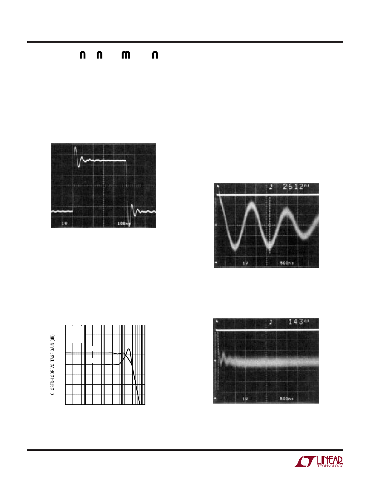
The LT1191 is quite tolerant of power supply bypassing. In
some applications a 0.1µF ceramic disc capacitor placed
1/2 inch from the amplifier is all that is required. A scope
photo of the amplifier output with no supply bypassing is
used to demonstrate this bypassing tolerance, RL = 1kΩ.
No Supply Bypass Capacitors
In most applications, and those requiring good settling
time, it is important to use multiple bypass capacitors. A
0.1µF ceramic disc in parallel with a 4.7µF tantalum is
recommended. Two oscilloscope photos with different
bypass conditions are used to illustrate the settling time
characteristics of the amplifier. Note that although the
output waveform looks acceptable at 1V/DIV, when ampli-
fied to1mV/DIV the settling time to 2mV is 2.61µs for the
0.1µF bypass; the time drops to 143ns with multiple
bypass capacitors.
Settling Time Poor Bypass
AV = –1, IN DEMO BOARD, RL = 1kΩ
LT1191 • TA04
Supply bypassing can also affect the response in the
frequency domain. It is possible to see a slight rise in the
frequency response at 130MHz depending on the gain
configuration, supply bypass, inductance in the supply
leads and printed circuit board layout. This can be further
minimized by not using a socket.
VOUT
1V/DIV
0V
Closed-Loop Voltage Gain vs Frequency
20
VS = ±5V
TA = 25°C
RL = 1k
10
AV = 2
AV = 1
0
VOUT
1V/DIV
0V
0V
VOUT
1mV/DIV
SETTLING TIME TO 2mV, AV = –1
SUPPLY BYPASS CAPACITORS = 0.1µF
LT1191 • TA06
Settling Time Good Bypass
0V
VOUT
1mV/DIV
–10
–20
100k
1M
10M
100M
1G
FREQUENCY (Hz)
LT1191 • TA05
LT1191 • TA07
SETTLING TIME TO 2mV, AV = –1
SUPPLY BYPASS CAPACITORS = 0.1µF + 4.7µF TANTALUM
8
Share Link: 