LT1227C 데이터 시트보기 (PDF) - Linear Technology
부품명
상세내역
제조사
LT1227C Datasheet PDF : 12 Pages
| |||
LT1227
APPLICATI S I FOR ATIO
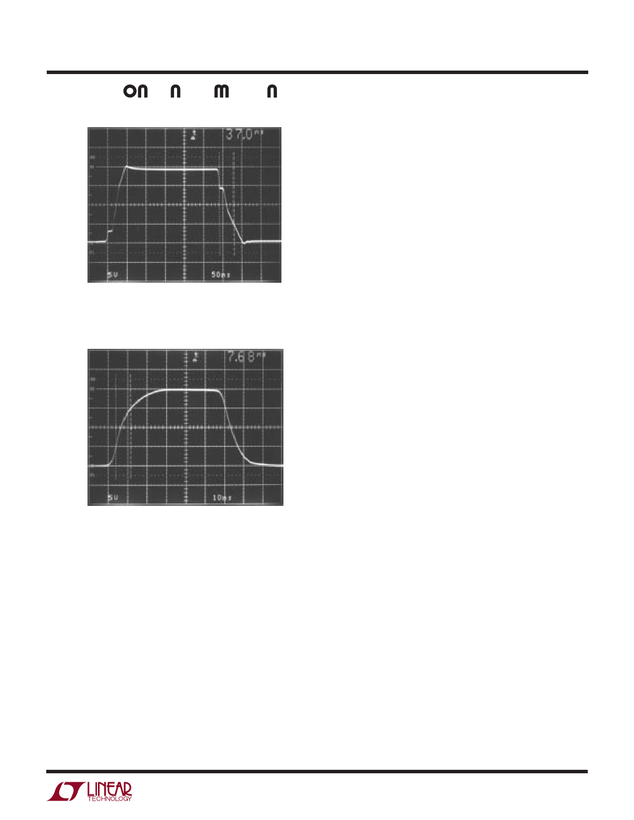
Large-Signal Transient Response, AV = +2
VOUT
RF = 1k, RG= 1k, RL = 400Ω
AI03
Large-Signal Transient Response, AV = –2
Shutdown
The LT1227 has a high impedance, low supply current
mode which is controlled by Pin 8. In the shutdown mode,
the output looks like a 12pF capacitor and the supply
current drops to approximately the Pin 8 current. The
shutdown pin is referenced to the positive supply through
an internal pullup circuit (see the simplified schematic).
Pulling a current of greater than 50µA from Pin 8 will put
the device into the shutdown mode. An easy way to force
shutdown is to ground Pin 8, using open drain (collector)
logic. Because the pin is referenced to the positive supply,
the logic used should have a breakdown voltage of greater
than the positive supply voltage. No other circuitry is
necessary as an internal JFET limits the Pin 8 current to
about 100µA. When Pin 8 is open, the LT1227 operates
normally.
VOUT
AI04
RF = 1k, RG= 510Ω, RL = 400Ω
AI04
Settling Time
The characteristic curves show that the LT1227 amplifier
settles to within 10mV of final value in 40ns to 55ns for any
output step up to 10V. The curve of settling to 1mV of final
value shows that there is a slower thermal contribution up
to 20µs. The thermal settling component comes from the
output and the input stage. The output contributes just
under 1mV per volt of output change and the input
contributes 300µV per volt of input change. Fortunately
the input thermal tends to cancel the output thermal. For
this reason the noninverting gain of two configuration
settles faster than the inverting gain of one.
Differential Input Signal Swing
The differential input swing is limited to about ±6V by an
ESD protection device connected between the inputs. In
normal operation, the differential voltage between the
input pins is small, so this clamp has no effect; however,
in the shutdown mode, the differential swing can be the
same as the input swing. The clamp voltage will then set
the maximum allowable input voltage. To allow for some
margin, it is recommended that the input signal be less
than ±5V when the device is shutdown.
Offset Adjust
Pins 1 and 5 are provided for offset nulling. A small current
to V+ or ground will compensate for DC offsets in the
device. The pins are referenced to the positive supply (see
the simplified schematic) and should be left open if un-
used. The offset adjust pins act primarily on the inverting
input bias current. A 10k pot connected to Pins 1 and 5
with the wiper connected to V+ will null out the bias
current, but will not affect the offset voltage much. Since
the output offset is
VO ≅ AV • VOS + (IIN–) • RF
at higher gains (AV > 5), the VOS term will dominate. To null
out the VOS term, use a 10k pot between Pins 1 and 5 with
a 150k resistor from the wiper to ground for 15V split
supplies, 47k for 5V split supplies.
9
Share Link: 