LT1374-5 데이터 시트보기 (PDF) - Linear Technology
부품명
상세내역
제조사
LT1374-5 Datasheet PDF : 28 Pages
| |||
LT1374
APPLICATIONS INFORMATION
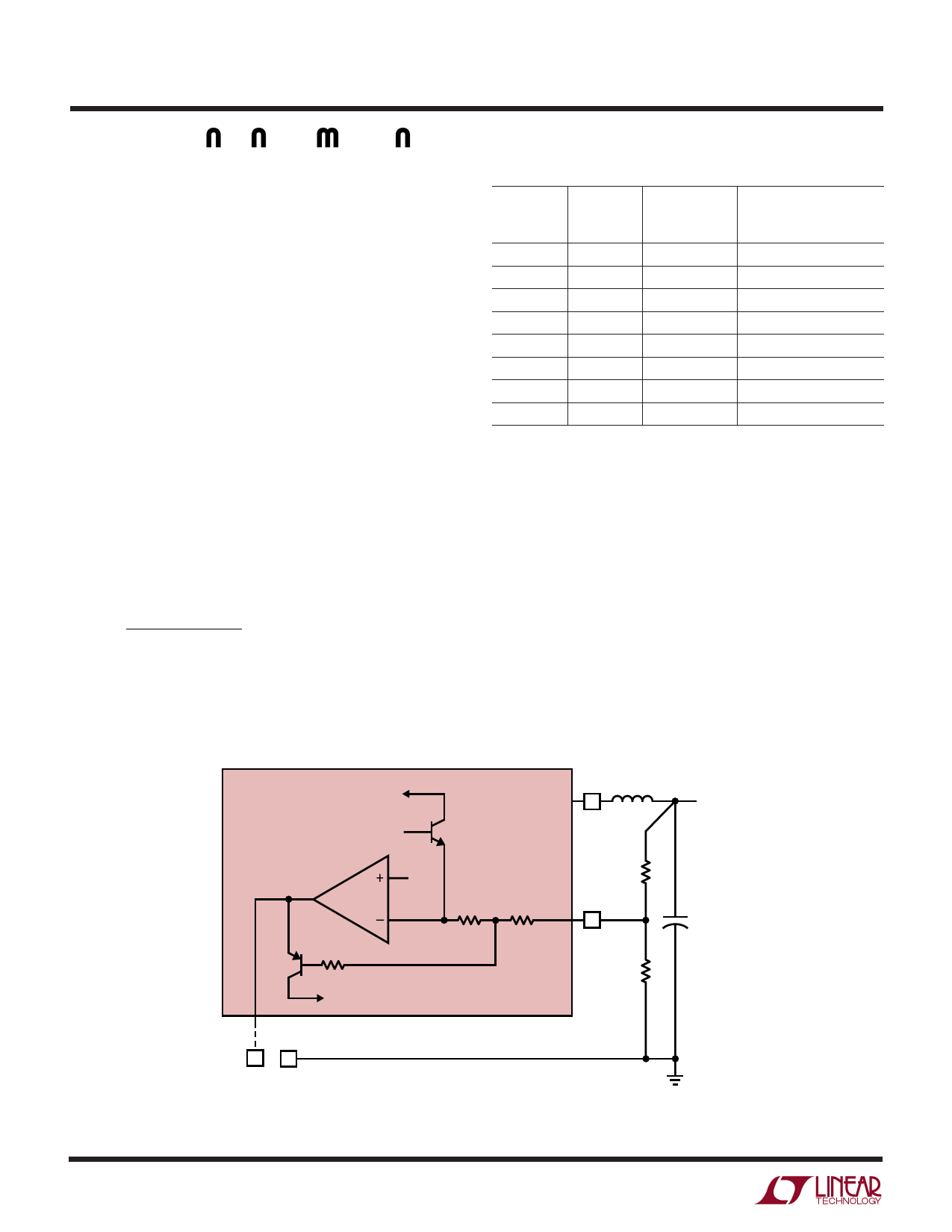
FEEDBACK PIN FUNCTIONS
The feedback (FB) pin on the LT1374 is used to set output
voltage and provide several overload protection features.
The first part of this section deals with selecting resistors
to set output voltage and the remaining part talks about
foldback frequency and current limiting created by the FB
pin. Please read both parts before committing to a final
design. The fixed 5V LT1374-5 has internal divider resis-
tors and the FB pin is renamed SENSE, connected directly
to the output.
The suggested value for the output divider resistor (see
Figure 2) from FB to ground (R2) is 5k or less, and a
formula for R1 is shown below. The output voltage error
caused by ignoring the input bias current on the FB pin is
less than 0.25% with R2 = 5k. A table of standard 1%
values is shown in Table 1 for common output voltages.
Please read the following if divider resistors are increased
above the suggested values.
( ) R1= R2 VOUT − 2.42
2.42
Table 1
OUTPUT
VOLTAGE
(V)
3
3.3
5
6
8
10
12
15
R1
% ERROR AT OUTPUT
R2
(NEAREST 1%) DUE TO DISCREET 1%
(kΩ)
(kΩ)
RESISTOR STEPS
4.99
1.21
+ 0.23
4.99
1.82
+ 0.08
4.99
5.36
+ 0.39
4.99
7.32
– 0.5
4.99
11.5
– 0.04
4.99
15.8
+ 0.83
4.99
19.6
– 0.62
4.99
26.1
+ 0.52
More Than Just Voltage Feedback
The feedback pin is used for more than just output voltage
sensing. It also reduces switching frequency and current
limit when output voltage is very low (see the Frequency
Foldback graph in Typical Performance Characteristics).
This is done to control power dissipation in both the IC and
in the external diode and inductor during short-circuit
conditions. A shorted output requires the switching regu-
lator to operate at very low duty cycles, and the average
current through the diode and inductor is equal to the
short-circuit current limit of the switch (typically 6A for the
LT1374, folding back to less than 3A). Minimum switch on
LT1374
TO FREQUENCY
SHIFTING
VSW
OUTPUT
5V
1.6V
Q1
ERROR
AMPLIFIER
2.4V
R3
R4
1k
1k
R1
FB
+
R5
5k
Q2
R2
5k
TO SYNC CIRCUIT
VC GND
1374 F02
Figure 2. Frequency and Current Limit Foldback
8
Share Link: 