LT1950 데이터 시트보기 (PDF) - Linear Technology
부품명
상세내역
제조사
LT1950 Datasheet PDF : 20 Pages
| |||
LT1950
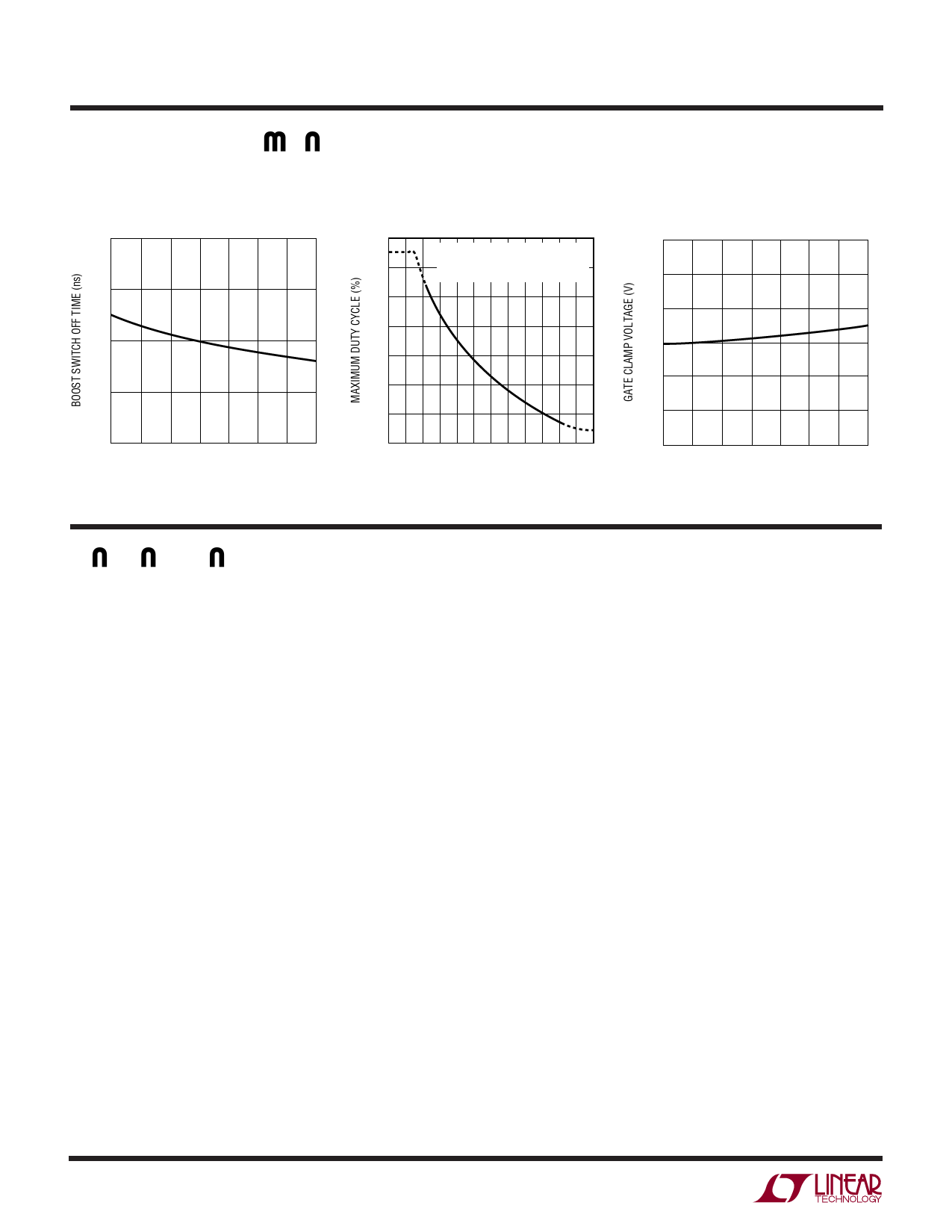
TYPICAL PERFOR A CE CHARACTERISTICS
BOOST Switch Off Time vs
Temperature
700
600
500
400
300
–50 –25
0 25 50 75
TEMPERATURE (°C)
100 125
1950 G16
Maximum Duty Cycle vs
VSEC Voltage
100
MAX DUTY CYCLE = (105/VSEC)%
90
1.25V < VSEC < 2.8V
TA = 25°C
80
70
60
50
40
30
0.8 1.2 1.6 2.0 2.4 2.8 3.2
VSEC VOLTAGE (V)
1950 G17
GATE Clamp Voltage vs
Temperature
16
15
14
13
12
11
10
–50 –25
0 25 50 75
TEMPERATURE (°C)
100 125
1950 G18
PI FU CTIO S
COMP (Pin 1): The COMP pin is the output of the error
amplifier. The error amplifier is a true op amp which allows
the use of an RC network to be connected between the
Comp and FB pins to compensate the feedback loop for
optimum transient response. The peak switch current in
the external MOSFET will be proportional to the voltage on
the COMP pin. Typical operating voltage range for this pin
is 1V to 2.5V.
FB (Pin 2): The FB pin is the inverting input to the error
amplifier. The output voltage is set with a resistor divider.
The error amplifier adjusts the peak switch current to
maintain the FB pin voltage at the value of the internal
reference voltage of 1.23V.
ROSC (Pin 3): A resistor from the ROSC pin to ground
programs the operating frequency of the LT1950. Operat-
ing frequency range is 100kHz to 500kHz. Nominal voltage
on the ROSC pin is 1V.
SYNC (Pin 4): The SYNC pin is used to synchronize the
internal oscillator to an external clock signal. The pin is
directly logic compatible and can be driven with any signal
with a duty cycle of 10% to 90%. If the SYNC function is
not used the pin can be left open circuit or connected to
ground.
SLOPE (Pin 5): The SLOPE pin is used to adjust the
amount of slope compensation. Leaving the pin open
circuit results in a default level of slope compensation. The
amount of slope compensation can be adjusted above this
default level by connecting a resistor from the SLOPE pin
to the VREF pin.
VREF (Pin 6): The VREF pin is the output of an internal 2.5V
reference. This pin is capable of sourcing up to 2.5mA for
external use. It is recommended that the VREF pin is
bypassed to ground with a 0.1µF ceramic capacitor.
SHDN (Pin 7): The SHDN pin is used to put the device into
a low power shutdown state. In shutdown the VIN supply
current drops to 5µA. The SHDN pin has an accurate
threshold of 1.32V which can be used to program an
undervoltage lockout threshold. Input current levels on
the SHDN pin can be used to program hysteresis into the
undervoltage lockout levels.
GND (Pin 8): The GND pin is the analog ground for the
internal circuitry of the LT1950. Sensitive circuitry such as
the feedback divider, frequency setting resistor, reference
bypass capacitor should be tied directly to this pin. See the
Applications Information section for recommendations
on ground connections.
1950fa
6
Share Link: 