LT1952EGN(RevD) 데이터 시트보기 (PDF) - Linear Technology
부품명
상세내역
제조사
LT1952EGN Datasheet PDF : 24 Pages
| |||

LT1952/LT1952-1
ELECTRICAL CHARACTERISTICS The l denotes the specifications which apply over the full operating
temperature range, otherwise specifications are at TA = 25°C. COMP = open, FB = 1.4V, ROSC = 178k, SYNC = 0V, SS_MAXDC = VREF, VREF
= 0.1μF, SD_VSEC = 2V, BLANK = 121k, DELAY = 121k, ISENSE = 0V, OC = 0V, OUT = 1nF, VIN = 15V, SOUT = open, unless otherwise specified.
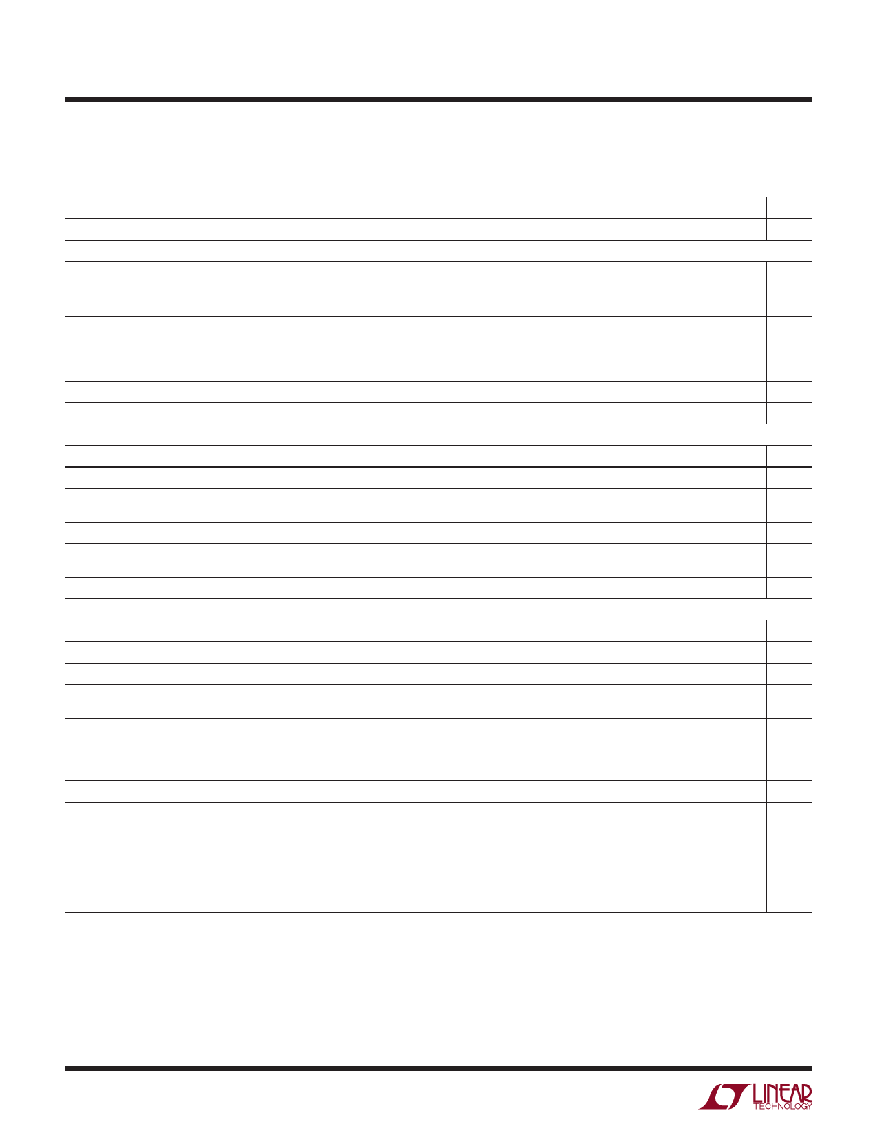
PARAMETER
SOUT DRIVER
CONDITIONS
MIN TYP MAX UNITS
SOUT Clamp Voltage
SOUT Low Level
SOUT High Level
SOUT Active Pull-Off in Shutdown
SOUT to OUT (Rise) DELAY (tDELAY)
VDELAY
OUT DRIVER
I(GATE) = 0μA, COMP = 2.5V, FB = 1V
I(GATE) = 25mA
I(GATE) = –25mA, VIN = 12V, COMP = 2.5V,
FB = 1V
VIN = 5V, SD_VSEC = 0V, SOUT = 1V
COMP = 2.5V, FB = 1V (Note 10)
RDELAY = 120k
10.5
12
13.5
V
0.5
0.75
V
10
V
1
mA
40
ns
120
ns
0.9
V
OUT Rise Time
FB = 1V, CL = 1nF (Notes 3, 6)
50
ns
OUT Fall Time
FB = 1V, CL = 1nF (Notes 3, 6)
30
ns
OUT Clamp Voltage
OUT Low Level
OUT High Level
OUT Active Pull-Off in Shutdown
OUT Max Duty Cycle
OUT Max Duty Cycle Clamp
SOFT-START
I(GATE) = 0μA, COMP = 2.5V, FB = 1V
I(GATE) = 20mA
I(GATE) = 200mA
I(GATE) = –20mA, VIN = 12V, COMP = 2.5V,
FB = 1V
I(GATE) = –200mA, VIN = 12V, COMP = 2.5V,
FB = 1V
VIN = 5V, SD_VSEC = 0V, OUT = 1V
COMP = 2.5V, FB = 1V, RDELAY = 10k
(fOSC = 200kHz), VIN = 10V
SD_VSEC = 1.4V, SS_MAXDC = VREF
COMP = 2.5V, FB = 1V, RDELAY = 10k
(fOSC = 200kHz), VIN = 10V
SD_VSEC = 1.32V, SS_MAXDC = 1.84V
SD_VSEC = 2.64V, SS_MAXDC = 1.84V
11.5
13
14.5
V
0.45 0.75
V
1.25
1.8
V
9.9
V
9.75
V
20
mA
83
90
%
63.5
72
80.5
%
25
33
41
%
SS_MAXDC Low Level: VOL
SS_MAXDC Soft-Start Reset Threshold
I(SS_MAXDC) = 150μA, OC = 1V
Measured on SS_MAXDC
0.2
V
0.45
V
SS_MAXDC Active Threshold
FB = 1V, DC > 0%
0.8
V
SS_MAXDC Input Current (Soft-Start Pull-Down: Idis) SS_MAXDC = 1V, SD_VSEC = 1.4V, OC = 1V
800
μA
Note 1: Stresses beyond those listed under Absolute Maximum Ratings
may cause permanent damage to the device. Exposure to any Absolute
Maximum Rating condition for extended periods may affect device
reliability and lifetime.
Note 2: The LT1952EGN/LT1952EGN-1 are guaranteed to meet
performance specifications from 0°C to 125°C junction temperature.
Specifications over the –40°C to 125°C operating junction temperature
range are assured by design, characterization and correlation with
statistical process controls. The LT1952IGN/LT1952IGN-1 are guaranteed
over the full –40°C to 125°C operating junction temperature range.
Note 3: Rise and Fall times are measured at 10% and 90% levels.
Note 4: Guaranteed by correlation to static test.
Note 5: Each IC includes over-temperature protection that is intended
to protect the device during momentary overload conditions. Junction
temperature will exceed 125°C when over-temperature protection is active.
Continuous operation above the specified maximum operating junction
temperature may impair device reliability.
Note 6: Guaranteed but not tested.
Note 7: Maximum recommended SYNC frequency = 500kHz.
Note 8: In applications where the VIN pin is supplied via an external RC
network from a SYSTEM VIN > 25V, an external zener with clamp voltage
VIN ON(MAX) < VZ < 25V should be connected from the VIN pin to ground.
Note 9: VIN start-up current is measured at VIN = VIN ON – 0.25V and
scaled by x 1.18 (to correlate to worst case VIN start-up current at VIN ON).
Note 10: Timing for R = 40k derived from measurement with R = 240k.
19521fd
4