LT3582 데이터 시트보기 (PDF) - Linear Technology
부품명
상세내역
제조사
LT3582
Linear Technology

LT3582 Datasheet PDF : 28 Pages
| |||
LT3582/LT3582-5/LT3582-12
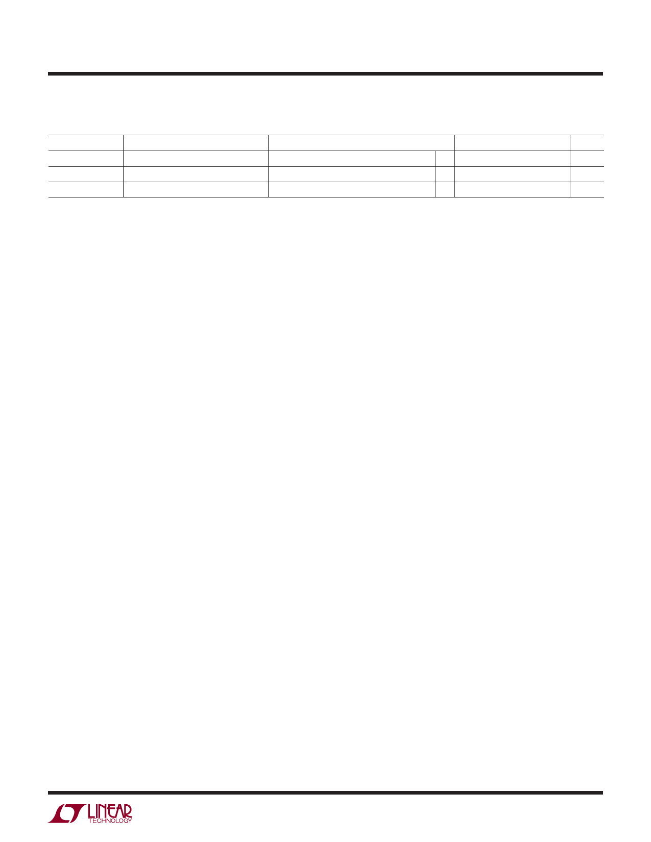
ELECTRICAL CHARACTERISTICS The l denotes the specifications which apply over the full operating
temperature range, otherwise specifications are at TA = 25°C. VIN = 3.6V, VSHDN = VIN unless otherwise noted. (Note 3)
I2C Timing Characteristics
SYMBOL
PARAMETER
CONDITIONS
MIN TYP MAX UNITS
tHD,DATRCV
tSU,DAT
tF
Data Hold Time Receiving
Data Setup Time
SDA Fall Time
LT3582 Receiving Data from Host
400pF load, VIN ≥ 2.5V
l
0
l 250
l
ns
ns
250
ns
Note 1: Stresses beyond those listed under Absolute Maximum Ratings
may cause permanent damage to the device. Exposure to any Absolute
Maximum Rating condition for extended periods may affect device
reliability and lifetime.
Note 2: LT3582 only.
Note 3: The LT3582E is guaranteed to meet performance specifications
from 0°C to 125°C junction temperature. Specifications over the –40°C
to 125°C operating junction temperature range are assured by design,
characterization and correlations with statistical process controls.
Note 4: These specifications apply to the VP trim bits in REG0 using
a 50mV LSB and do not include the additional VPLUS trim bit. See
Registers and OTP in the Applications Information section.
Note 5: This IC includes over-temperature protection that is intended
to protect the device during momentary overload conditions. Junction
temperature will exceed the maximum operating junction temperature
when over-temperature protection is active. Continuous operation above
the specified maximum operating junction temperature may impair
device reliability.
Note 6: Output voltage is measured under non-switching test conditions
approximating a moderate load current from the output.
3582512f
5
Share Link: