LT3587 데이터 시트보기 (PDF) - Linear Technology
부품명
상세내역
제조사
LT3587 Datasheet PDF : 24 Pages
| |||
LT3587
APPLICATIONS INFORMATION
capacitance will slow down the switching waveform, which
can cause significant switching losses at 1MHz switch-
ing frequency. Some recommended Schottky diodes are
listed in Table 2.
Table 2. Recommended Schottky Diodes
PART
NUMBER
DIODE
FORWARD FORWARD CAPACI-
CURRENT VOLTAGE TANCE
(mA) DROP (V) (pF at 10V) MANUFACTURER
RSX051VA-30 1000
0.35
30
ROHM
www.rohm.com
PMEG401OCEJ 500
0.49
PMEG2005EB
500
0.43
25
NXP/Phillips
8
www.nxp.com
IR05H40CSPTR 500
0.48
39
Vishay
www.vishay.com
B0540WS
500
0.48
20
Diodes Inc.
www.diodes.com
ZLLS400
520
0.53
17
Zetex
www.zetex.com
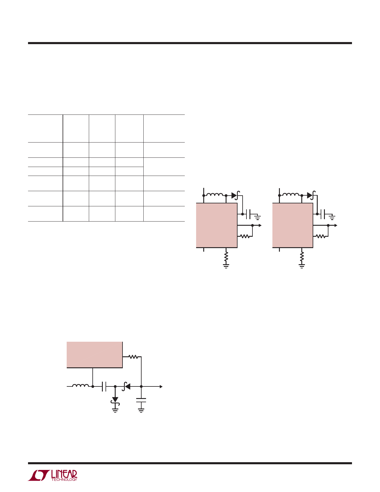
Smaller Footprint Inverter Topology
In certain applications with higher tolerance of current ripple
at the output of the inverter, the inductor L3 can be replaced
with a Schottky diode. Since the Schottky diode footprint
is usually smaller than the inductor footprint, this alternate
topology is recommended if a smaller overall solution is a
must. Note that this topology is only viable if the absolute
value of the inverter output is greater than VIN.
This Schottky diode is configured with the anode connected
to the output of the inverter and the cathode to the output
end of the flying capacitor C2 as shown in Figure 2.
VVIN
2.5V TO 4.5V
LT3587
RFB1
1M
FB2
SW2
L2
15μH
3587 F02
C2
2.2μF
D3
INVERTER
OUTPUT
–8V, 100mA
DS2
C7
22μF
Figure 2. Inverter Configured with a Schottky
Diode in Place of the Output Inductor
The same constraints as the other Schottky diodes ap-
ply for selecting D3. Therefore, the same recommended
Schottky diodes in Table 2 can be used for D3.
Boost3 Overcurrent and Overvoltage Protection
As briefly discussed in the Operation section, the regula-
tion loop of Boost3 uses the maximum of the two voltages
at VFB3 and IFB3 as feedback information to set the peak
current of its power switch Q3. This allows for the Boost3
loop to be configured as either a boost voltage regulator
or a boost current regulator (Figure 3). Furthermore, this
architecture also allows for a programmable current limit on
voltage regulation or voltage limit on current regulation.
VVIN
VVIN
VIN
SW3
VIN
SW3
CAP3
LT3587
BOOST3
VOLTAGE
VOUT3
REGULATOR
VFB3
EN/SS3
IFB3
RVFB3
VOLTAGE
REGULATION
FEEDBACK
RIFB3 RESISTOR
CAP3
LT3587
BOOST3
CURRENT
VOUT3
REGULATOR
VFB3
EN/SS3
IFB3
RVFB3
OPTIONAL
PROGRAMMABLE
VOLTAGE LIMIT
RIFB3 RESISTOR
OPTIONALPROGRAMMABLE
CURRENT LIMIT RESISTOR
CURRENT REGULATION
FEEDBACK RESISTOR
3587 F03
Figure 3. Boost3 Configured as a Voltage
Regulator and as a Current Regulator
When configured as a boost voltage regulator, a feedback
resistor from the output pin VOUT3 to the VFB3 pin sets the
voltage level at VOUT3 at a fixed level. In this case, the IFB3
pin can either be grounded if no current limiting is desired
or connected to ground with a resistor such that:
ILIMIT = 200 • (0.8V/RIFB3)
where ILIMIT is the desired output current limit value. Recall
that the pull-up current on the IFB3 pin is controlled to be
typically 1/200 of the output load current at the VOUT3
pin. In this case, when the load current is less than ILIMIT,
the Boost3 loop regulates the voltage at the VFB3 pin to
0.8V. When there is an increase in load current beyond
ILIMIT, the voltage at VFB3 starts to drop and the voltage
at IFB3 rises above 0.8V. The Boost3 loop then regulates
the voltage at the IFB3 pin to 0.8V, limiting the output
3587fc
11
Share Link: 