LT3954IUHE 데이터 시트보기 (PDF) - Linear Technology
부품명
상세내역
제조사
LT3954IUHE Datasheet PDF : 26 Pages
| |||
LT3954
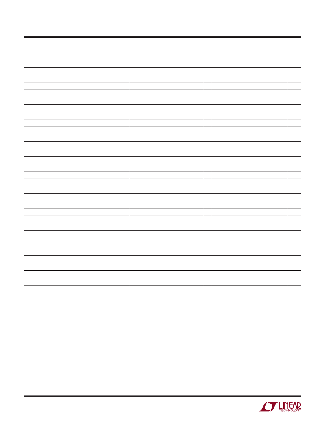
ELECTRICAL CHARACTERISTICS The l denotes the specifications which apply over the full operating
temperature range, otherwise specifications are at TA = 25°C. VIN = 24V, EN/UVLO = 24V, CTRL = 2V, PWM = 5V, unless otherwise noted.
PARAMETER
CONDITIONS
MIN
TYP
MAX UNITS
Linear Regulator
INTVCC Regulation Voltage
INTVCC Maximum Operating Voltage
INTVCC Minimum Operating Voltage
Dropout (VIN – INTVCC)
INTVCC Undervoltage Lockout
INTVCC Current Limit
INTVCC Current in Shutdown
Logic Inputs/Outputs
10V ≤ VIN ≤ 40V
IINTVCC = –10mA, VIN = 7V
8V ≤ VIN ≤ 40V, INTVCC = 6V
EN/UVLO = 0V, INTVCC = 8V
l 7.60
7.85
8.05
V
8.1
V
4.5
V
390
mV
l
3.9
4.1
4.4
V
30
36
42
mA
8
13
µA
EN/UVLO Threshold Voltage Falling
l 1.180
1.220
1.260
V
EN/UVLO Rising Hysteresis
40
mV
EN/UVLO Input Low Voltage
EN/UVLO Pin Bias Current Low
IVIN Drops Below 1µA
EN/UVLO = 1.15V
0.4
V
1.7
2.2
2.7
µA
EN/UVLO Pin Bias Current High
EN/UVLO = 1.33V
10
100
nA
VMODE Output Low
VMODE Pin Leakage
IVMODE = 1mA
FB = 0V, VMODE = 12V
200
mV
0.1
5
µA
PWM Pin Signal Generator
PWM Falling Threshold
l 0.78
0.83
0.88
V
PWM Threshold Hysteresis (VPWMHYS)
PWM Pull-Up Current (IPWMUP)
PWM Pull-Down Current (IPWMDN)
PWM Fault-Mode Pull-Down Current
PWMOUT Duty Ratio for PWM Signal Generator (Note 5)
PWMOUT Signal Generator Frequency
PWMOUT Driver
IDIM/SS = 0µA
PWM = 0.7V, IDIM/SS = 0µA
PWM = 1.5V, IDIM/SS = 0µA
INTVCC = 3.6V
IDIM/SS = –6.5µA
IDIM/SS = 0µA
IDIM/SS = 21.5µA
IDIM/SS = 52µA
PWM = 47nF to GND, IDIM/SS = 0µA
0.35
0.47
0.6
V
6
7.5
9
µA
68
88
110
µA
1.5
mA
3.1
4.1
5.2
%
6.2
7.9
9.2
%
40
48
56
%
95
96.5
98
%
170
300
390
Hz
PWMOUT Driver Output Rise Time (tr)
PWMOUT Driver Output Fall Time (tf)
PWMOUT Output Low (VOL)
PWMOUT Output High (VOH)
CL = 560pF
CL = 560pF
PWM = 0V
35
35
INTVCC – 0.05
ns
ns
0.05
V
V
Note 1: Stresses beyond those listed under Absolute Maximum Ratings
may cause permanent damage to the device. Exposure to any Absolute
Maximum Rating condition for extended periods may affect device
reliability and lifetime.
Note 2: Do not apply a positive or negative voltage or current source to
PWMOUT pin, otherwise permanent damage may occur.
Note 3: The LT3954E is guaranteed to meet performance specifications
from the 0°C to 125°C junction temperature. Specifications over the –40°C
to 125°C operating junction temperature range are assured by design,
characterization and correlation with statistical process controls. The
LT3954I is guaranteed over the full –40°C to 125°C operating junction
temperature range.
Note 4: The LT3954 includes overtemperature protection that is intended
to protect the device during momentary overload conditions. Junction
temperature will exceed the maximum operating junction temperature
when overtemperature protection is active. Continuous operation above
the specified maximum junction temperature may impair device reliability.
Note 5: PWMOUT Duty Ratio is calculated:
Duty = IPWMUP/(IPWMUP + IPWMDN)
3954fa
4
For more information www.linear.com/3954
Share Link: 