LT5521 데이터 시트보기 (PDF) - Linear Technology
부품명
상세내역
제조사
LT5521 Datasheet PDF : 16 Pages
| |||
LT5521
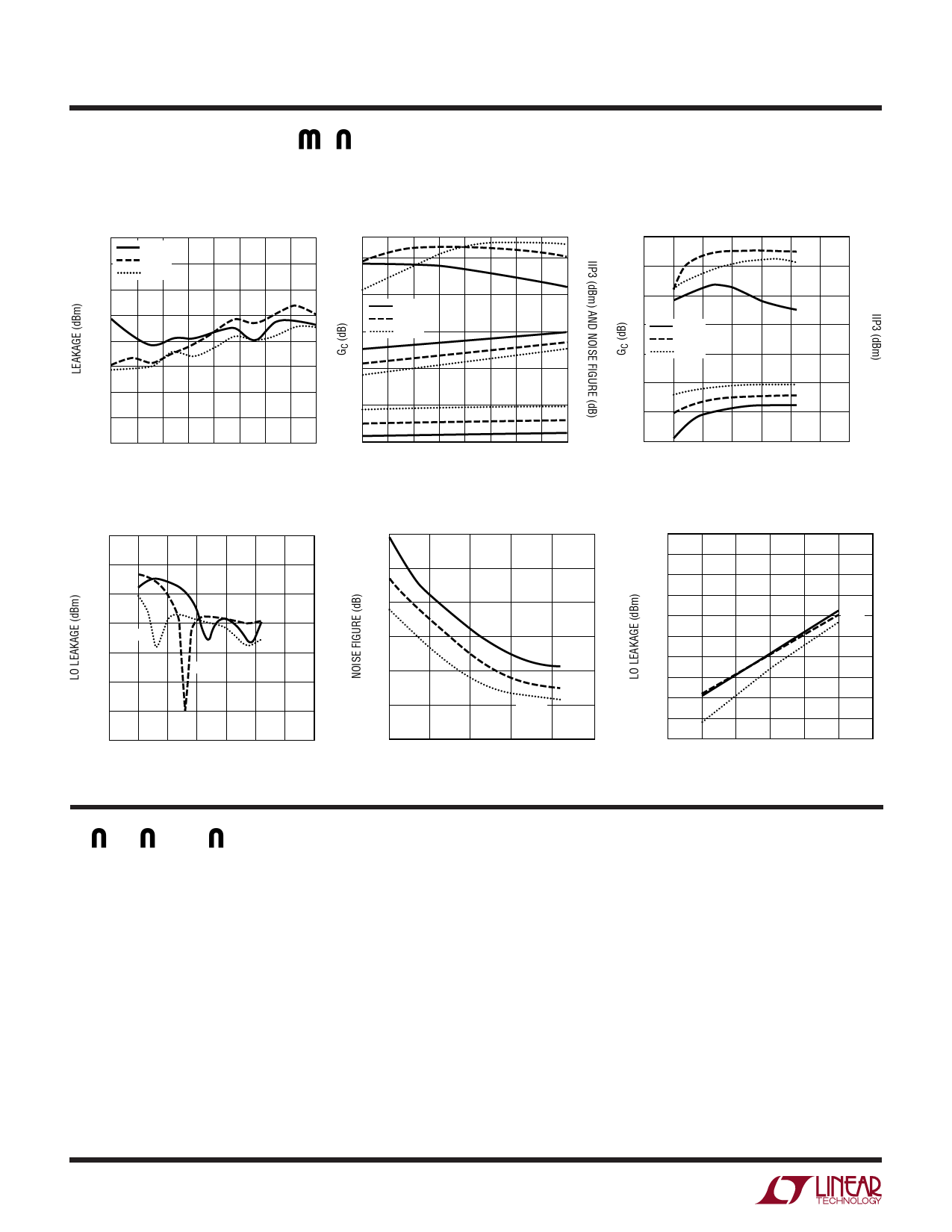
TYPICAL AC PERFOR A CE CHARACTERISTICS fLO = 1.7GHz, fIF = 250MHz, fRF = 1.95GHz, PLO
= –5dBm, VCC = 3.3V, EN = 2.9V, TA = 25°C, unless otherwise noted. Test circuit shown in Figure 1 is tuned for 1.95GHz output
frequency and VCC = 3.3V.
LO-RF Leakage vs LO Frequency
Conversion Gain, IIP3 and Noise
Figure vs Supply Voltage
Conversion Gain and IIP3
vs LO Power
–32
85°C
–33
25°C
–40°C
–34
–35
–36
–37
–38
–39
8
6
85°C
25°C
4
–40°C
2
0
GC
10
24
IIP3
8
20
6
27
25
IIP3
23
NF
16
4
85°C
25°C
21
2
–40°C
19
12
0
GC
17
8
–2
15
–40
1500 1550 1600 1650 1700 1750 1800 1850 1900
LO FREQUENCY (MHz)
5521 G28
–2
4
3.10 3.15 3.20 3.25 3.30 3.35 3.40 3.45 3.50
VCC (V)
5521 G31
–4
–25 –20 –15 –10 –5 0
LO POWER (dBm)
13
5 10
5521 G29
LO-RF Leakage vs LO Power
–30
–32
85°C
–34
–36
–40°C
–38
25°C
–40
–42
–44
–25 –20
–15 –10 –5 0
LO POWER (dBm)
5 10
5521 G30
Noise Figure vs LO Power
22
20
18
16
85°C
14
25°C
12
–40°C
10
–20
–15 –10
–5
LO POWER (dBm)
0
5
5521 G32
LO Leakage vs Supply Voltage
–20
–23
–26
–29
–32
85°C 25°C
–35
–40°C
–38
–41
–44
–47
–50
3.0 3.1 3.2 3.3 3.4 3.5 3.6
VCC (V)
5521 G33
PI FU CTIO S
GND (Pins 1, 4, 10, 11, 13, 14, 16): Ground. These pins
are internally connected to the Exposed Pad for improved
isolation. They should be connected to RF ground on the
printed circuit board, and are not intended to replace the
primary grounding through the backside of the package.
IN+, IN– (Pins 2, 3): Differential Input Pins. Each pin
requires a resistive DC path to ground. See Applications
Information for choosing the resistor value. External match-
ing is required.
EN (Pin 5): Enable Input Pin. The enable voltage should be
at least 2.9V to turn the chip on and less than 0.2V to turn
the chip off.
8
VCC (Pins 6, 7, 8): Power Supply Pins. Total current draw
for these three pins is 40mA.
OUT+, OUT– (Pins 12, 9): RF Output Pins. These pins must
have a DC connection to the supply voltage (see Applica-
tions Information). These pins draw 20mA each. External
matching is required.
LO (Pin 15): Local Oscillator Input. This input is internally
DC biased to 0.96V. Input signal must be AC coupled.
Exposed Pad (Pin 17): Circuit Ground Return for the
Entire IC. For best performance, this pin must be soldered
to the printed circuit board.
5521f
Share Link: 