LTC1059M(RevD) 데이터 시트보기 (PDF) - Linear Technology
부품명
상세내역
제조사
LTC1059M Datasheet PDF : 8 Pages
| |||
LTC1059
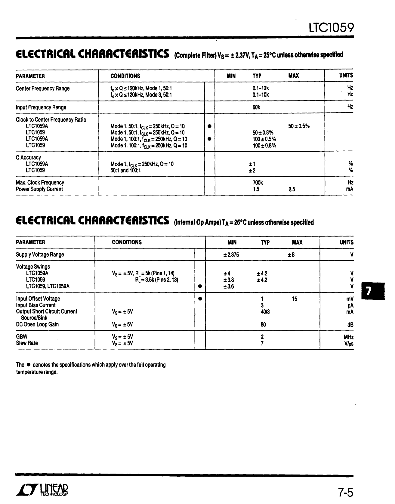
ELECTRICAL CHARACTERISTICS The ● denotes the specifications which apply over the full operating
temperature range, otherwise specifications are at TA = 25°C.
(Complete Filter) VS = ±5V, T2L Clock Input Level unless otherwise specified.
PARAMETER
DC Lowpass Gain Accuracy
BP Gain Accuracy at f0
Clock Feedthrough
Max Clock Frequency
Power Supply Current
CONDITIONS
Mode 1, R1 = R2 = 50kΩ
Mode 1, Q = 10, f0 = 5kHz
fCLK ≤ 1MHz
Mode 1, Q < 5, VS ≥ ±5V
MIN TYP MAX UNITS
●
±0.1
2
%
±0.1
%
10
mV
2
MHz
3.5
5.5
mA
●
7
mA
(Complete Filter) VS = ±2.37V unless otherwise specified.
PARAMETER
Center Frequency Range
Input Frequency Range
Clock-to-Center Frequency Ratio
Q Accuracy
Max Clock Frequency
Power Supply Current
CONDITIONS
f0 • Q ≤ 120kHz, Mode 1, 50:1
f0 • Q ≤ 120kHz, Mode 3, 50:1
Mode 1, 50:1, fCLK = 250kHz, Q = 10
Mode 1, 100:1, fCLK = 250kHz, Q = 10
Mode 1, fCLK = 250kHz, Q = 10
50:1 and 100:1
MIN TYP MAX
0.1 - 12k
0.1 - 10k
60k
UNITS
Hz
Hz
Hz
50 ± 0.8%
100 ± 0.8%
±2
%
700
kHz
1.5
2.5
mA
(Internal Op Amps) The ● denotes the specifications which apply over the full operating temperature range,
otherwise specifications are at TA = 25°C.
PARAMETER
Supply Voltage Range
Voltage Swings
Input Offset Voltage
Input Bias Current
Output Short-Circuit Current Source/Sink
DC Open Loop Gain
GBW
Slew Rate
CONDITIONS
VS = ±5V, RL = 5k (Pins 1, 14)
RL = 3.5k (Pins 2, 13)
VS = ±5V (N Package)
VS = ±5V (S Package)
VS = ±5V
VS = ±5V
VS = ±5V
MIN TYP
±2.375
±3.8 ±4.2
● ±3.6
●
1
3
40/3
25/3
80
2
7
MAX UNITS
±8
V
V
V
15
mV
pA
mA
mA
dB
MHz
V/µs
Note 1: Absolute Maximum Ratings are those values beyond which the life
of a device may be impaired.
1059fd
3
Share Link: 