LTC1152 데이터 시트보기 (PDF) - Linear Technology
부품명
상세내역
제조사
LTC1152 Datasheet PDF : 8 Pages
| |||
LTC1152
APPLICATI S I FOR ATIO
Rail-to-Rail Operation
The LTC1152 is a rail-to-rail input common-mode range,
rail-to-rail output swing op amp. Most CMOS op amps,
including the entire LTC zero-drift amplifier line, and even
a few bipolar op amps, can and do, claim rail-to-rail output
swing. One obvious use for such a device is to provide a
unity-gain buffer for 0V to 5V signals running from a single
5V power supply. This is not possible with the vast
majority of so-called “rail-to-rail” op amps; although the
output can swing to both rails, the negative input (which
is connected to the output) will exceed the common-mode
input range of the device at some point (generally about
1.5V below the positive supply), opening the feedback
loop and causing unpredictable and sometimes bizarre
behavior.
The LTC1152 is an exception to this rule. It features both
rail-to-rail output swing and rail-to-rail input common-
mode range (CMR); the input CMR actually extends be-
yond either rail by about 0.3V. This allows unity-gain
buffer circuits to operate with any input signal within the
power supply rails; input signal swing is limited only by the
output stage swing into the load. Additionally, signals
occurring at either rail (power supply current sensing, for
example) can be amplified without any special circuitry.
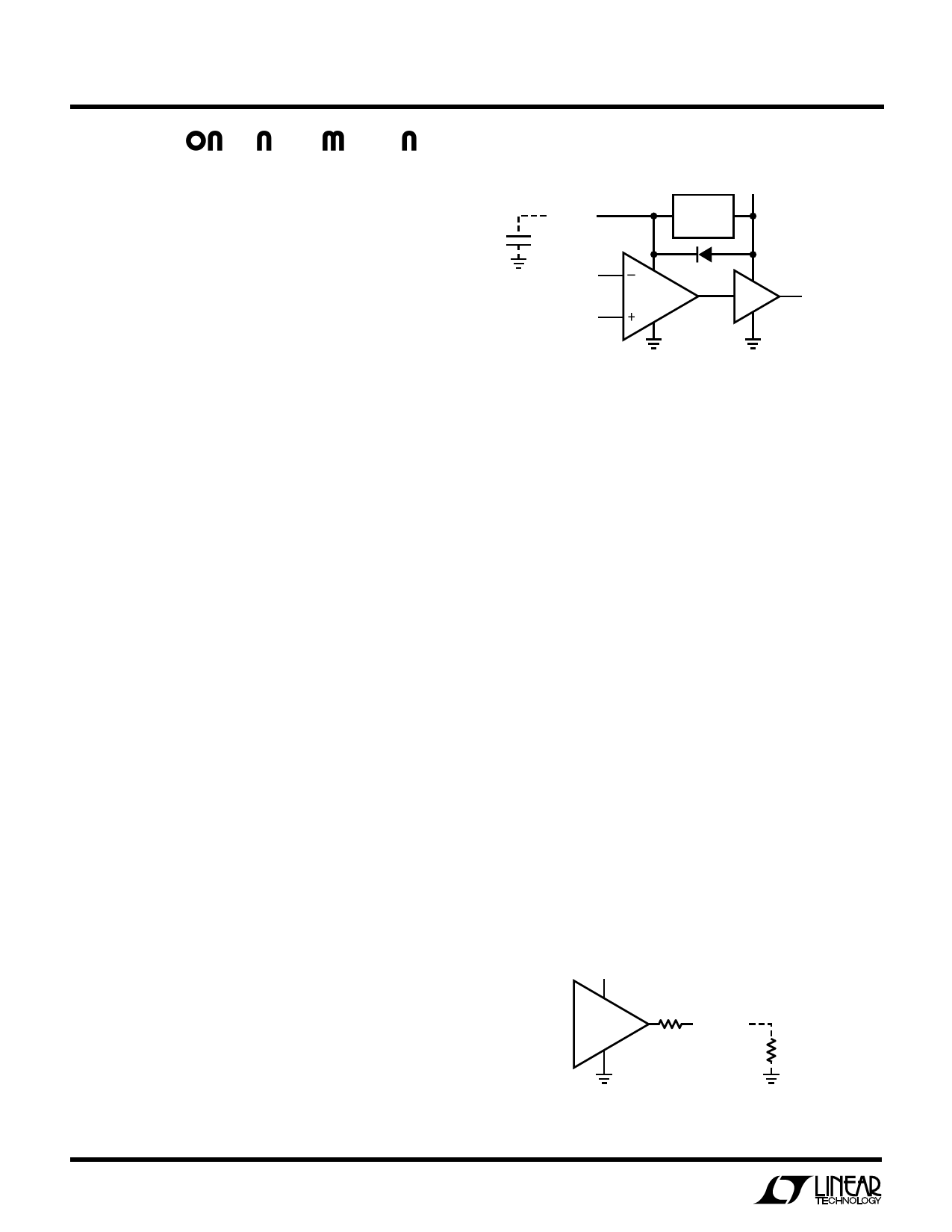
Internal Charge Pump
The LTC1152 achieves its rail-to-rail input CMR by using
a charge pump to generate an internal voltage approxi-
mately 2V higher than V +. The input stages of the op amp
are run from this higher voltage, making signals at V+
appear to be 2V below the front end’s power supply (Figure
1). The charge pump is contained entirely within the
LTC1152; no external components are required.
About 100µVP-P of residual charge pump switching noise
will be present on the output of the LTC1152. This
feedthrough is at 4.7MHz, higher than the gain-bandwidth
of the LTC1152, and will generally not cause any prob-
lems. Very sensitive applications can reduce this
feedthrough by connecting a capacitor from the CP pin
(pin 8) to V+(pin 7); a 0.1µF capacitor will reduce charge
pump feedthrough to negligible levels. The LTC1152 in-
cludes an internal diode from pin 8 to pin 7 to prevent
external parasitic capacitance from lengthening start-up
VCC + 2V
CP (PIN 8)
0.1µF*
VCC
(PIN 7)
INTERNAL
CHARGE
PUMP
–
–IN
INPUT
OUT
+
+IN
*OPTIONAL EXTERNAL
CAPACITOR TO REDUCE
CHARGE PUMP FEEDTHROUGH
OUTPUT
RAIL TO RAIL
1152 F01
Figure 1. LTC1152 Internal Block Diagram
time. This diode can stand short-term peak currents of
about 50mA, allowing it to quickly charge external capaci-
tance to ground or V –. Large capacitors (>1µF) should not
be connected between pin 8 and ground or V – to prevent
excessive diode current from flowing at start-up. The
LTC1152 can withstand continuous short circuits be-
tween pin 8 and V +; however, short circuiting pin 8 to
ground or V – will cause large amounts of current to flow
through the diode, destroying the LTC1152. Don’t do it.
Output Drive
The LTC1152 features an enhanced output stage that can
sink and source 10mA with a single 5V supply while
maintaining rail-to-rail output swing under most loading
conditions. The output stage can be modeled as a perfect
rail-to-rail voltage source with a resistor in series with it;
this open-loop output resistance limits the output swing
by creating a resistor divider with the output load.
The output resistance drops as total power supply voltage
increases, as shown in the typical performance curves. It
is typically 140Ω with a single 5V supply, allowing a 4.4V
output swing into a 1k resistor with a single 5V supply.
VCC (PIN 7)
LTC1152
OUTPUT
DRIVER
ROUT
OUT (PIN 6)
≈140Ω AT 5V SUPPLY
RLOAD
1152 F02
Figure 2. LTC1152 Output Resistance Model
6
Share Link: 