LCX034ALT 데이터 시트보기 (PDF) - Sony Semiconductor
부품명
상세내역
제조사
LCX034ALT Datasheet PDF : 26 Pages
| |||
LCX034ALT
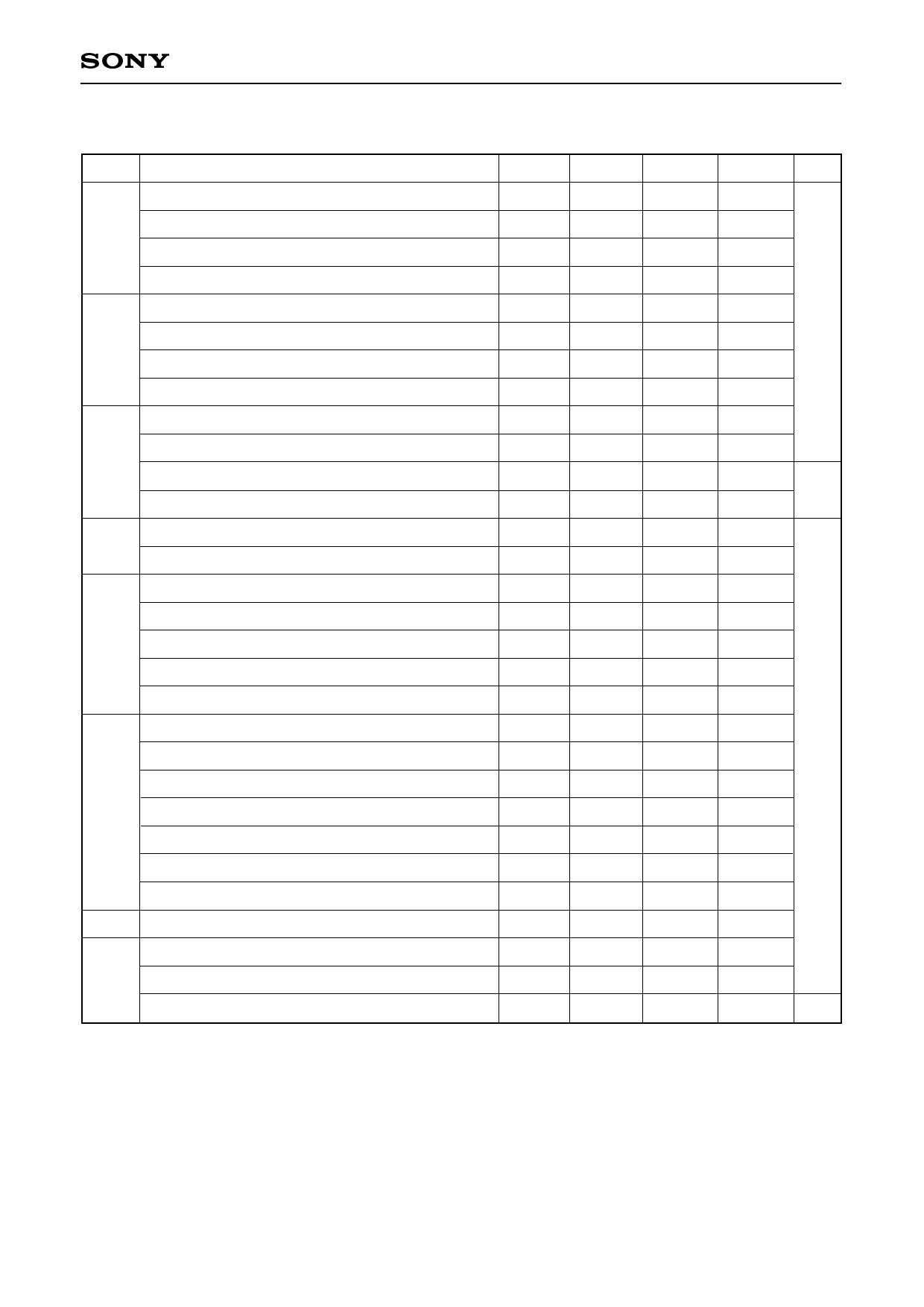
2. Clock timing conditions (Ta = 25°C)
(SVGA mode: fHCKn = 4.0MHz, fVCK = 24.0kHz)
Item
Symbol Min.
Typ.
Max. Unit
Hst rise time
trHst
—
—
30
Hst fall time
HST
Hst data set-up time
tfHst
—
—
30
tdHst
50
60
70
HCK
Hst data hold time
Hckn rise time∗5
Hckn fall time∗5
Hck1 fall to Hck2 rise time
Hck1 rise to Hck2 fall time
thHst
50
60
trHckn
—
—
tfHckn
—
—
to1Hck –15
0
to2Hck –15
0
70
30
ns
30
15
15
Vst rise time
trVst
—
—
100
Vst fall time
VST
Vst data set-up time
Vst data hold time
tfVst
—
tdVst
5
thVst
5
—
100
10
15
µs
10
15
Vck rise time
VCK
Vck fall time
trVck
—
tfVck
—
—
100
—
100
Enb rise time
trEnb
—
—
100
Enb fall time
tfEnb
—
—
100
ENB Vck rise/fall to Enb rise time
toEnb
300
500
—
Horizontal video period completed to Enb fall time tdEnb
900
1000
—
Enb fall to Pcg rise time
toPcg
630
700
—
Pcg rise time
trPcg
—
—
30
Pcg fall time
tfPcg
—
—
30
ns
Pcg rise to Prg rise time
toPrgr
300
500
—
PCG Pcg rise to Prg rise time
toPrgf
200
250
—
Prg rise to Pcg fall time
toPcg
1050
1100
—
Pcg fall to horizontal video period start time
toVideo 300
350
—
Pcg pulse width
twPcg 1350
1600
—
PRG Prg rise to Vck rise/fall time
toVck
0
1000
—
Blk rise time
BLK∗6 Blk fall time
trBlk
—
—
100
tfBlk
—
—
100
Blk fall to Vst rise time
toVst
32
—
—
µs
∗5 Hckn means Hck1 and Hck2.
∗6 Blk is set to positive polarity pulse for other than SVGA mode ; Low level for SVGA mode.
–7–
Share Link: 