LTC1726IS8-2.5(RevB) 데이터 시트보기 (PDF) - Linear Technology
부품명
상세내역
제조사
LTC1726IS8-2.5
(Rev.:RevB)
(Rev.:RevB)
Linear Technology

LTC1726IS8-2.5 Datasheet PDF : 12 Pages
| |||
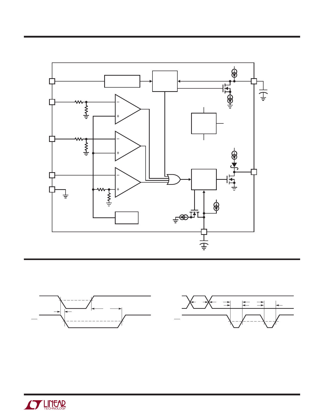
LTC1726
APPLICATIO S I FOR ATIO
Supply Monitoring
The LTC1726 is a low power, high accuracy triple supply
monitor and watchdog timer. The watchdog and reset
periods are both adjustable using external capacitors.
All three VCC inputs must be above predetermined thresh-
olds for reset not to be asserted. The LTC1726 will assert
reset during power-up, power-down and brownout condi-
tions on any one or all of the VCC inputs.
Upon power-up, either the VCC5/VCC25 or VCC3 pin can
power the drive circuits for the RST pin. This ensures that
RST will be low when either VCC5/VCC25 or VCC3 reaches
1V. As long as any one of the VCC inputs is below its
predetermined threshold, RST will stay a logic low. Once
all of the VCC inputs rise above their thresholds, the
adjustable reset timer is started and RST is released after
the reset time-out period.
On power-down, once any of the VCC inputs drops below its
threshold, RST is held at a logic low. A logic low of 0.3V is
guaranteed until both VCC3 and VCC5/VCC25 drop below 1V.
3V or 5V/2.5V Power Detect
Since the LTC1726 is a multisupply monitor, it will be
required to assert reset as soon as there is power on any
one of the monitor inputs. Therefore, the part derives its
power from either the VCC3 or VCC5/VCC25 input, which-
ever pin has the greatest potential. This ensures the part
pulls the RST pin low as soon as either input pin is ≥1V.
The adjustable input is excluded from being a potential
supply pin because of its 1V nominal operating range.
Override Functions (5V Versions Only)
The VCCA pin, if unused, can be tied to either VCC3 or VCC5.
This is an obvious solution since the trip points for VCC3
and VCC5 will always be greater than the trip point for VCCA.
The VCC5 input trip point is disabled if its voltage is equal
to the voltage on VCC3 ±25mV and the voltage on VCC5 is
less than 4.15V. In this manner the LTC1726-5 behaves
as a 3.3V monitor and the 5V reset function is disabled.
The VCC5 trip point is re-enabled when the voltage on
VCC5 is equal to the voltage on VCC3 ±25mV and the two
inputs are greater than approximately 4.15V. In this
manner, the part can function as a 5V monitor with the
3.3V monitor disabled.
When monitoring either 3.3V or 5V with VCC3 strapped to
VCC5, (see Figure 1) the part determines which is the
appropriate range. The part handles this situation as
shown in Figure 2. Above 1V and below VRT3, RST is held
low. From VRT3 to approximately 4.15V, the part as-
sumes 3.3V supply monitoring and RST is deasserted.
Above approximately 4.15V, the part operates as a 5V
monitor. In most systems, the 5V supply will pass
through the 3.1V to 4.15V region in < 200ms during
power-up, and the RST output will behave as desired.
Table 1 summarizes the state of RST at various operating
voltages with VCC3 = VCC5.
Table 1. Override Truth Table (VCC3 = VCC5)
INPUTS (VCC3 = VCC5 = VCC)
RST
0V ≤ VCC ≤ 1V
—
1V ≤ VCC ≤ VRT3
0
VRT3 ≤ VCC ≤ 4.15V
1
4.15V ≤ VCC ≤ VRT5
0
VRT5 ≤ VCC
1
VCC
3.3V OR 5V
LTC1726-5
1
VCC3
2
VCC5
3
VCCA
6
RST
4
GND
R1
10k
TO SYSTEM
RESET
1726 F01
PINS 5, 7 AND 8 NOT SHOWN FOR CLARITY
Figure 1. Single Supply Monitor with Others Disabled
5
VCC3 = VCC5 = VCCA = 0V TO 5V
10k PULL-UP FROM RST TO VCC3
4 TA = 25°C
3
2
1
0
0
1
2
3
4
5
SUPPLY VOLTAGE (V)
1726 F02
Figure 2. RST Voltage vs Supply Voltage
1726fb
7
Share Link: