LTC5536 데이터 시트보기 (PDF) - Linear Technology
부품명
상세내역
제조사
LTC5536 Datasheet PDF : 12 Pages
| |||
LTC5536
APPLICATIO S I FOR ATIO
Operation
The LTC5536 is configured as a fast detector and high
speed comparator for RF power detection and RF power
alarms. The product integrates several functions to pro-
vide RF power detection over frequencies ranging from
600MHz to 7GHz. These functions include an RF Schottky
diode peak detector, a level shift amplifier to convert the RF
input signal to low frequency, and a fast comparator. The
LTC5536 provides a comparator reference input VM and a
latch enable input LEN.
RF Detector
The internal RF Schottky diode peak detector and level
shift amplifier convert the RF input signal to a low fre-
quency signal. The detector demonstrates excellent effi-
ciency and linearity over a wide range of input power. The
Schottky diode is biased at about 55µA, and drives a 15pF
internal peak detector capacitor.
High Speed Comparator
The fast internal comparator compares the external refer-
ence voltage at VM to the internal signal voltage from the
peak detector, and produces the output signal, VOUT. The
internal peak detector voltage is factory trimmed to 100mV
with no RF signal present. The comparator has approxi-
mately 10mV of hysteresis, with a typical VOUT low-to-high
switching point of 100mV and a VOUT high-to-low switch-
ing point of 90mV with no RF signal present.
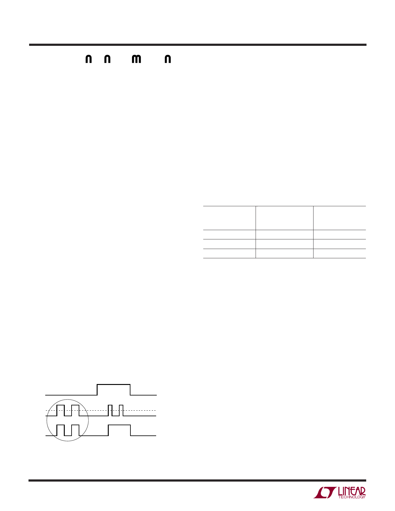
The comparator also has a built-in latch. This will cause the
VOUT output to latch high on a positive comparator transi-
tion (increasing RF power), when the LEN pin is high, as
indicated in the waveforms of Figure 1. For transparent
LEN
VM
VP
VOUT
VOUT
TRANSPARENT
VOUT
LATCHED
EXTERNAL
ENABLE
OUTPUT
RF DET
OUTPUT OF
COMPARATOR
VOUT
TRANSPARENT
5536 AI01
operation of the comparator (no latching action), the LEN
pin should be connected to ground.
The comparator output (VOUT) rise and fall times are
approximately 2ns (unloaded). The propagation delay for
the comparator alone was characterized by applying a
continuous 2GHz RF signal to the RFIN input. Then a 1MHz
square wave (0V to 2.5V) was applied to the VM input to
switch the comparator. Note that there is a signal inver-
sion, because the VM pin is connected internally to the
negative comparator input. The time delay from the tran-
sition edge of the square wave at the VM input to the
corresponding VOUT output transition (rising or falling) is
shown in Table 1.
Table 1. Comparator Propagation Delay
RF Input
Level
(dBm)
VOUT Rising
Edge Delay
(ns)
–10
38.5
0
24
10
20
VOUT Falling
Edge Delay
(ns)
36
40
86
Overall Propagation Delay and Response Time
Figure 2 shows measurements of total propagation delay
from the RFIN signal input to the VOUT output of the
LTC5536, plotted as a function of RF input power. The
response is shown for RF Signal Absent-to-RF Signal
Present Transitions (Rising Edge VOUT), and for RF Signal
Present-to-RF Signal Absent Transitions (Falling Edge
VOUT). The LTC5536’s RF detector is optimized as a
positive peak detector. Consequently, the device responds
to a rising signal at the RF input much more rapidly than
to a falling signal. Correspondingly, Rising Edge VOUT
transitions are much more rapid than Falling Edge transi-
tions, as shown in Figure 2. The minimum propagation
delay is about 20ns at room temperature, in response to
strong overdrive conditions at the RFIN input. These
results were measured by applying a 1GHz RF signal that
was amplitude modulated by a 1MHz square wave with
50% duty cycle. An example time domain waveform is
shown in Figure 3.
Figure 1. LTC5536 LEN Function Waveform
5536f
8
Share Link: 