LTC6605-10 데이터 시트보기 (PDF) - Linear Technology
부품명
상세내역
제조사
LTC6605-10
Linear Technology

LTC6605-10 Datasheet PDF : 20 Pages
| |||
LTC6605-10
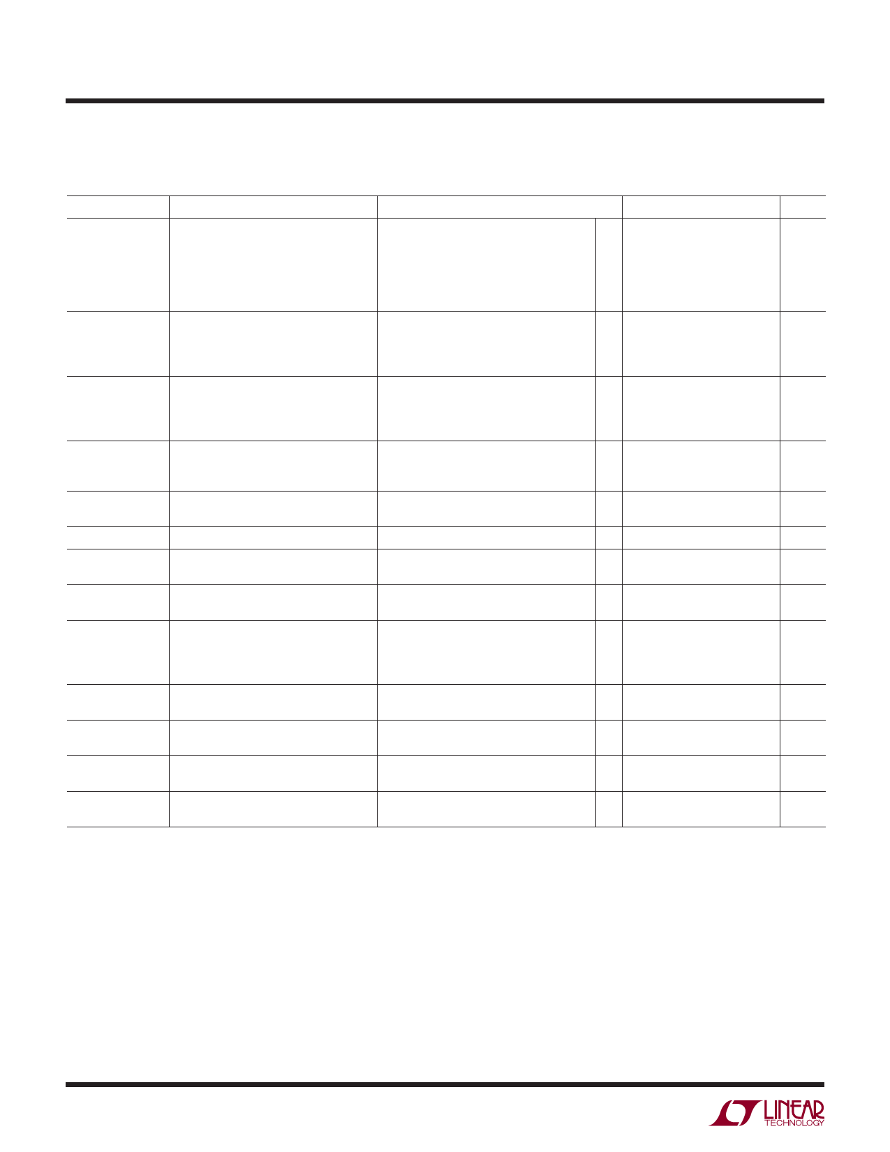
AC ELECTRICAL CHARACTERISTICS The l denotes the specifications which apply over the full operating
temperature range, otherwise specifications are at TA = 25°C. V+ = 3V, V– = 0V, VINCM = VOCM = mid-supply, VBIAS = V+, unless
otherwise noted. Filter configured as in Figure 2, unless otherwise noted. VS is defined as (V+ – V–). VOUTCM is defined as (V+OUT +
V–OUT)/2. VINCM is defined as (V+IN + V–IN)/2. VOUTDIFF is defined as (V+OUT – V–OUT). VINDIFF is defined as (V+IN + V–IN).
SYMBOL
PARAMETER
CONDITIONS
MIN TYP MAX UNITS
Gain
Phase
ΔGain
ΔPhase
4V/V Gain
Filter Gain
Filter Phase
Gain Match (Channel-to-Channel)
Phase Match (Channel-to-Channel)
Filter Gain in 4V/V Configuration
Inputs at ±IN1 Pins, ±IN4 Pins Floating
ΔVIN = ±0.125V, DC
VINDIFF = 0.5VP-P, f = 5MHz
VINDIFF = 0.5VP-P, f = 7.5MHz
VINDIFF = 0.5VP-P, f = 10MHz
VINDIFF = 0.5VP-P, f = 20MHz
VINDIFF = 0.5VP-P, f = 50MHz
ΔVIN = ±0.125V, DC
VINDIFF = 0.5VP-P, f = 5MHz
VINDIFF = 0.5VP-P, f = 7.5MHz
VINDIFF = 0.5VP-P, f = 10MHz
ΔVIN = ±0.125V, DC
VINDIFF = 0.5VP-P, f = 5MHz
VINDIFF = 0.5VP-P, f = 7.5MHz
VINDIFF = 0.5VP-P, f = 10MHz
VINDIFF = 0.5VP-P, f = 5MHz
VINDIFF = 0.5VP-P, f = 7.5MHz
VINDIFF = 0.5VP-P, f = 10MHz
ΔVIN = ±0.125V, DC
l –0.25 ±0.05 0.25
dB
l –1.1 –0.77 –0.4
dB
l –2.35 –1.89 –1.45
dB
l –4.05 –3.5
–3
dB
l –11.75 –11.1 –10.55
dB
l –28 –25.8 –24.8
dB
0
Deg
–42.5
Deg
–63.2
Deg
–81.7
Deg
l –0.2 ±0.05 0.2
dB
l –0.2 ±0.05 0.2
dB
l –0.3 ±0.05 0.3
dB
l –0.35 ±0.05 0.35
dB
l –1.1 ±0.2
1.1
Deg
l –1.2 ±0.2
1.2
Deg
l –1.2 ±0.2
1.2
Deg
l 11.85 12 12.25
dB
fO TC
Channel Separation
Filter Cut-Off Frequency Temperature
Coefficient
VINDIFF = 1VP-P, f = 5MHz
BIAS = V+
BIAS = Floating
–96
dB
–80
ppm/°C
–260
ppm/°C
Noise
en
in
HD2
HD3
Integrated Output Noise
(BW = 10kHz to 20MHz)
Input Referred Noise Density (f = 1MHz) BIAS = V+
Figure 4, Gain = 1
Figure 4, Gain = 4
Figure 4, Gain = 5
Voltage Noise Density Referred to
Op Amp Inputs (f = 1MHz)
BIAS = V+
BIAS = Floating
Current Noise Density Referred to
Op Amp Inputs (f = 1MHz)
BIAS = V+
BIAS = Floating
2nd Harmonic Distortion
fIN = 5MHz; VIN = 2VP-P Single-Ended
3rd Harmonic Distortion
fIN = 5MHz; VIN = 2VP-P Single-Ended
BIAS = V+
BIAS = Floating, RLOAD = 400Ω
BIAS = V+
BIAS = Floating, RLOAD = 400Ω
69
μVRMS
20
nV/√Hz
5
nV/√Hz
4
nV/√Hz
2.1
nV/√Hz
2.6
nV/√Hz
3
pA /√Hz
2.1
pA /√Hz
–90
dBc
–75
dBc
–106
dBc
–82
dBc
Note 1: Stresses beyond those listed under Absolute Maximum Ratings
may cause permanent damage to the device. Exposure to any Absolute
Maximum Rating condition for extended periods may affect device
reliability and lifetime.
Note 2: All pins are protected by steering diodes to either supply. If any
pin is driven beyond the LTC6605-10’s supply voltage, the excess input
current (current in excess of what it takes to drive that pin to the supply
rail) should be limited to less than 10mA.
Note 3: A heat sink may be required to keep the junction temperature
below the Absolute Maximum Rating when the output is shorted
indefinitely. Long-term application of output currents in excess of the
Absolute Maximum Ratings may impair the life of the device.
Note 4: Both the LTC6605C and the LTC6605I are guaranteed functional
over the operating temperature range –40°C to 85°C.
Note 5: The LTC6605C is guaranteed to meet specified performance
from 0°C to 70°C. The LTC6605C is designed, characterized and
expected to meet specified performance from –40°C to 85°C, but is
not tested or QA sampled at these temperatures. The LTC6605I is
guaranteed to meet specified performance from –40°C to 85°C.
Note 6: Output referred voltage offset is a function of gain. To determine
output referred voltage offset, or output voltage offset drift, multiply VOS
by the noise gain (1 + GAIN). See Figure 3.
Note 7: Input bias current is defined as the average of the currents
flowing into the noninverting and inverting inputs of the internal amplifier
and is calculated from measurements made at the pins of the IC. Input
offset current is defined as the difference of the currents flowing into
the noninverting and inverting inputs of the internal amplifier and is
calculated from measurements made at the pins of the IC.
660510f
4
Share Link: