TC1054-4.0VCT 데이터 시트보기 (PDF) - Microchip Technology
부품명
상세내역
제조사
TC1054-4.0VCT Datasheet PDF : 18 Pages
| |||
TC1054/TC1055/TC1186
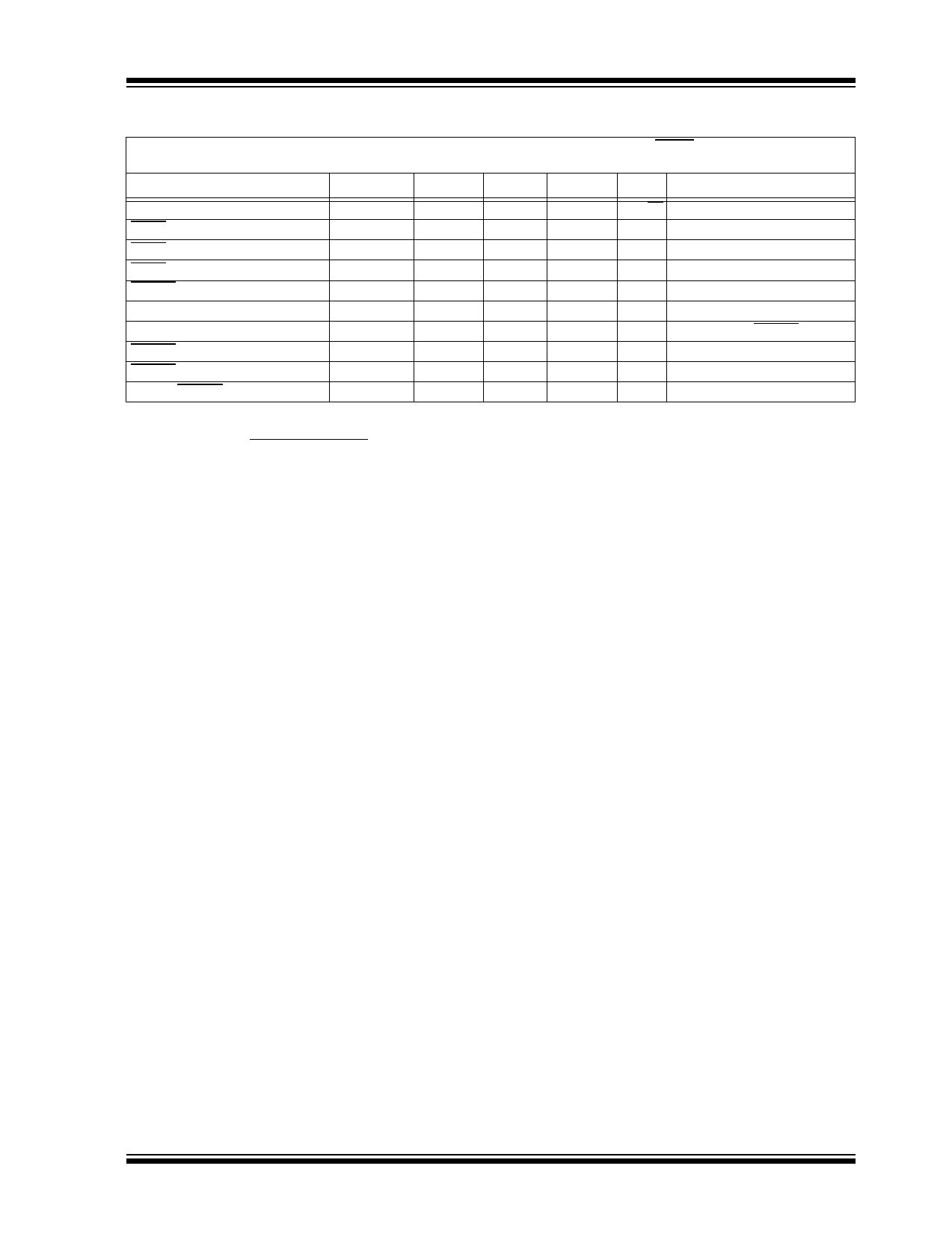
DC CHARACTERISTICS (CONTINUED)
Electrical Specifications: Unless otherwise noted, VIN = VOUT + 1V, IL = 100 µA, CL = 3.3 µF, SHDN > VIH, TA = +25°C.
Boldface type specifications apply for junction temperatures of -40°C to +125°C.
Parameters
Sym
Min
Typ
Max
Units
Conditions
Output Noise
SHDN Input
eN
—
260
—
nV/√Hz IL = IOUTMAX
SHDN Input High Threshold
SHDN Input Low Threshold
ERROR Output
VIH
45
—
—
%VIN VIN = 2.5V to 6.5V
VIL
—
—
15
%VIN VIN = 2.5V to 6.5V
Minimum VIN Operating Voltage
VINMIN
1.0
—
—
V
Output Logic Low Voltage
VOL
—
—
400
mV 1 mA Flows to ERROR
ERROR Threshold Voltage
VTH
—
0.95 x VR
—
V See Figure 4-2
ERROR Positive Hysteresis
VHYS
—
50
—
mV Note 7
VOUT to ERROR Delay
tDELAY
—
2.5
—
ms VOUT falling from VR to VR - 10%
Note 1: VR is the regulator output voltage setting. For example: VR = 1.8V, 2.5V, 2.7V, 2.85V, 3.0V, 3.3V, 3.6V, 4.0V, 5.0V.
2: TC VOUT = (VOUTMAX – VOUTMIN)x 106
VOUT x ΔT
3: Regulation is measured at a constant junction temperature using low duty cycle pulse testing. Load regulation is tested
over a load range from 0.1 mA to the maximum specified output current. Changes in output voltage due to heating
effects are covered by the thermal regulation specification.
4: Dropout voltage is defined as the input to output differential at which the output voltage drops 2% below its nominal
value.
5: Thermal Regulation is defined as the change in output voltage at a time T after a change in power dissipation is applied,
excluding load or line regulation effects. Specifications are for a current pulse equal to ILMAX at VIN = 6V for T = 10 ms.
6: The maximum allowable power dissipation is a function of ambient temperature, the maximum allowable junction
temperature and the thermal resistance from junction-to-air (i.e., TA, TJ, θJA). Exceeding the maximum allowable power
dissipation causes the device to initiate thermal shutdown. Please see Section 5.0 “Thermal Considerations”, “Ther-
mal Considerations”, for more details.
7: Hysteresis voltage is referenced by VR.
8: The minimum VIN has to justify the conditions: VIN ≥ VR + VDROPOUT and VIN ≥ 2.7V for IL = 0.1 mA to IOUTMAX.
9: Apply for junction temperatures of -40C to +85C.
© 2007 Microchip Technology Inc.
DS21350D-page 3
Share Link: 