M24C16-FCS6TP 데이터 시트보기 (PDF) - STMicroelectronics
부품명
상세내역
제조사
M24C16-FCS6TP Datasheet PDF : 39 Pages
| |||
M24C16, M24C08, M24C04, M24C02, M24C01
Device operation
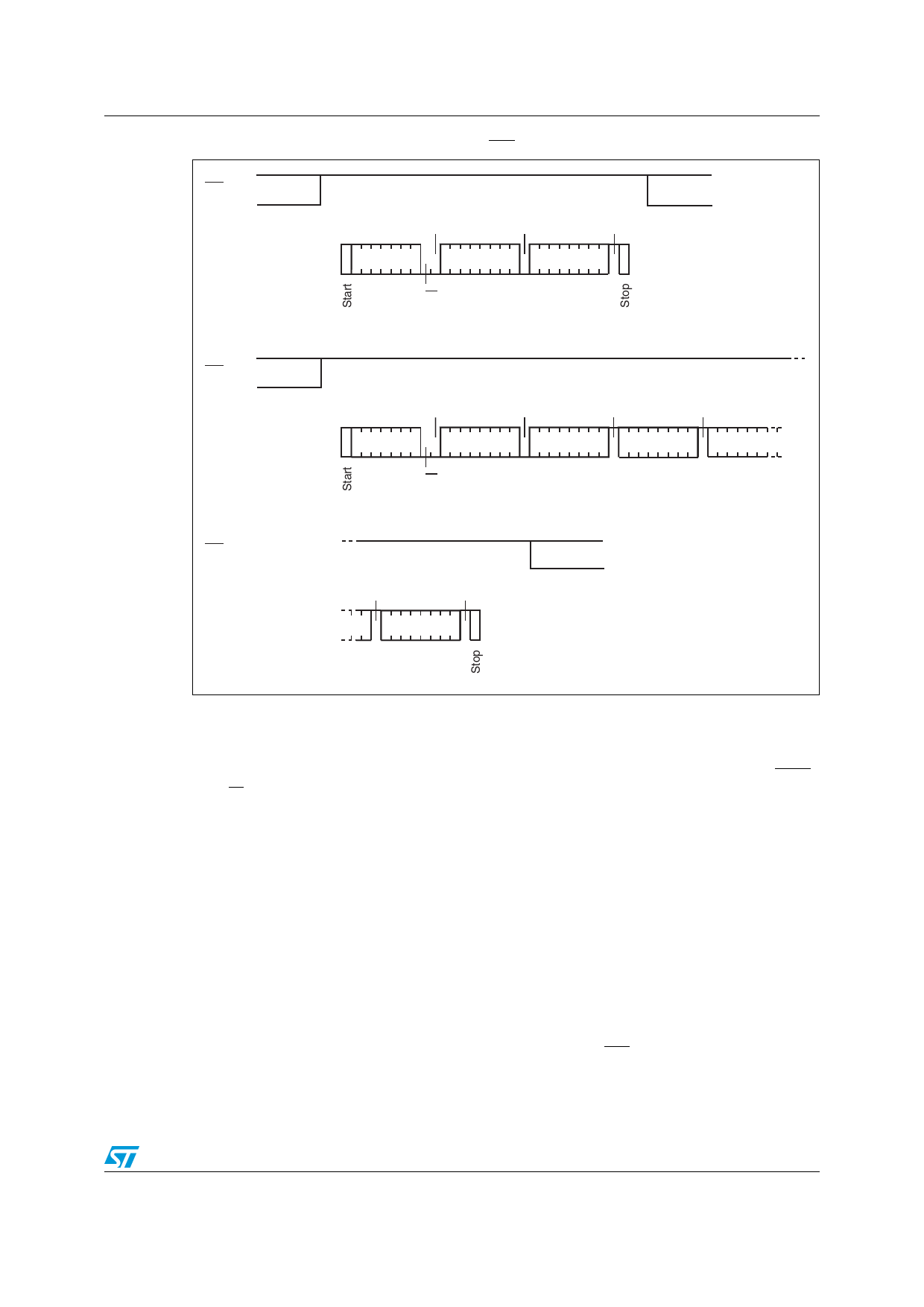
Figure 7. Write mode sequences with WC = 1 (data write inhibited)
WC
Byte Write
ACK
ACK
NO ACK
Dev select
Byte address
Data in
R/W
WC
Page Write
ACK
ACK
NO ACK
NO ACK
Dev select
Byte address
Data in 1
Data in 2
Data in 3
R/W
3.6
3.6.1
WC (cont'd)
Page Write
(cont'd)
NO ACK
NO ACK
Data in N
AI02803d
Write operations
Following a Start condition the bus master sends a device select code with the Read/Write
bit (RW) reset to 0. The device acknowledges this, as shown in Figure 8, and waits for an
address byte. The device responds to the address byte with an acknowledge bit, and then
waits for the data byte.
When the bus master generates a Stop condition immediately after a data byte’s Ack bit (in
the “10th bit” time slot), either at the end of a Byte Write or a Page Write, the internal write
cycle is triggered. A Stop condition at any other time slot does not trigger the internal write
cycle.
During the internal Write cycle, Serial Data (SDA) and Serial Clock (SCL) are ignored, and
the device does not respond to any requests.
Byte Write
After the device select code and the address byte, the bus master sends one data byte. If
the addressed location is Write-protected, by Write Control (WC) being driven High (during
the period from the Start condition until the end of the address byte), the device replies to
the data byte with NoAck, as shown in Figure 7, and the location is not modified. If, instead,
Doc ID 5067 Rev 16
13/39
Share Link: 